MC68HC908MR8

Features: • High-performance M68HC08 architecture• Fully upward-compatible object code with M6805, M146805, and M68HC05 Families• 8-MHz internal bus frequency• 8 Kbytes of on-chip FLASH• On-chip programming firmware for use with host personal computer• 256 bytes...

product image

MC68HC908MR8 Picture
SeekIC No. : 004416538 Detail

MC68HC908MR8: Features: • High-performance M68HC08 architecture• Fully upward-compatible object code with M6805, M146805, and M68HC05 Families• 8-MHz internal bus frequency• 8 Kbytes of on...

floor Price/Ceiling Price

Part Number:
MC68HC908MR8
Supply Ability:
5000

Price Break

  • Qty
  • 1~5000
  • Unit Price
  • Negotiable
  • Processing time
  • 15 Days
Total Cost: $ 0.00

SeekIC Buyer Protection PLUS - newly updated for 2013!

  • Escrow Protection.
  • Guaranteed refunds.
  • Secure payments.
  • Learn more >>

Month Sales

268 Transactions

Rating

evaluate  (4.8 stars)

Upload time: 2024/11/27

Payment Methods

All payment methods are secure and covered by SeekIC Buyer Protection PLUS.

Notice: When you place an order, your payment is made to SeekIC and not to your seller. SeekIC only pays the seller after confirming you have received your order. We will also never share your payment details with your seller.
Product Details

Description


Features:

• High-performance M68HC08 architecture
• Fully upward-compatible object code with M6805, M146805, and M68HC05 Families
• 8-MHz internal bus frequency
• 8 Kbytes of on-chip FLASH
• On-chip programming firmware for use with host personal computer
• 256 bytes of on-chip random-access memory (RAM):
• 12-bit, 6-channel center-aligned or edge-aligned pulse-width modulator (PWMMC)
• Serial communications interface module (SCI)
• Two 16-bit, 2-channel timer interface modules (TIMA and TIMB)
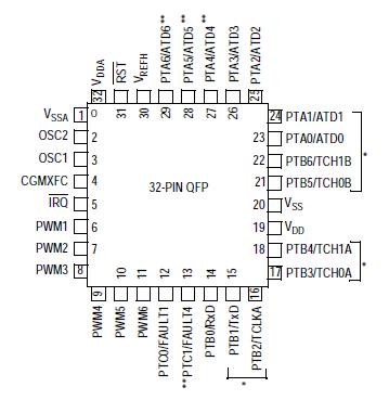
• Eight high current sink and source pins (PTA1/ATD1, PTA0/ATD0,PTB6/TCH1B, PTB5/TCH0B, PTB4/TCH1A, PTB3/TCH0A,PTB2/TCLKA, and PTB1/TxD)
• Clock generator module (CGM)
• Digitally filtered low-voltage inhibit (LVI), software selectable for ±5 percent or ±10 percent tolerance
• 10-bit, 4 to 7-channel analog-to-digital converter (ADC)
• System protection features:
Optional computer operating properly (COP) reset
Low-voltage detection with optional reset
Illegal opcode detection with optional reset
Illegal address detection with optional reset
Fault detection with optional PWM disabling
• Available packages:
32-pin low-profile quad flat pack (LQFP)
28-pin dual in-line package (PDIP)
28-pin small outline package (SOIC)
• Low-power design, fully static with stop and wait modes
• Break (BRK) module allows single breakpoint setting during in-circuit debugging
• Master reset pin and power-on reset (POR)


Pinout

  Connection Diagram


Specifications

Characteristic(1)
Symbol
Value
Unit
Supply Voltage
VDD
0.3 to +6.0
V
Input Voltage
VIN
VSS0.3 to VDD+0.3
V
Input high voltage
VHI
VDD+4
V
Maximum current per pin
excluding VDD and VSS
I
±25
°C
Storage temperature
tstg
55 to +150
mA
Maximum current out of VSS
IMVSS
100
mA
Maximum current into VDD
IMVDD
100
mA


Customers Who Bought This Item Also Bought

Margin,quality,low-cost products with low minimum orders. Secure your online payments with SeekIC Buyer Protection.
Transformers
Crystals and Oscillators
Connectors, Interconnects
Soldering, Desoldering, Rework Products
Cables, Wires - Management
Fans, Thermal Management
View more