MC68HC908LB8

Features: • 8-MHz internal bus frequency• Trimmable internal oscillator: 4.0 MHz internal bus operation 8-bit trim capability 25% untrimmed 5% trimmed• 8 Kbytes of 10 K write/erase cycle typical on-chip in application programmable FLASH memory with security option(1)• 128 b...

product image

MC68HC908LB8 Picture
SeekIC No. : 004416532 Detail

MC68HC908LB8: Features: • 8-MHz internal bus frequency• Trimmable internal oscillator: 4.0 MHz internal bus operation 8-bit trim capability 25% untrimmed 5% trimmed• 8 Kbytes of 10 K write/erase...

floor Price/Ceiling Price

Part Number:
MC68HC908LB8
Supply Ability:
5000

Price Break

  • Qty
  • 1~5000
  • Unit Price
  • Negotiable
  • Processing time
  • 15 Days
Total Cost: $ 0.00

SeekIC Buyer Protection PLUS - newly updated for 2013!

  • Escrow Protection.
  • Guaranteed refunds.
  • Secure payments.
  • Learn more >>

Month Sales

268 Transactions

Rating

evaluate  (4.8 stars)

Upload time: 2024/11/27

Payment Methods

All payment methods are secure and covered by SeekIC Buyer Protection PLUS.

Notice: When you place an order, your payment is made to SeekIC and not to your seller. SeekIC only pays the seller after confirming you have received your order. We will also never share your payment details with your seller.
Product Details

Description


Features:

• 8-MHz internal bus frequency
• Trimmable internal oscillator:
4.0 MHz internal bus operation
8-bit trim capability
25% untrimmed
5% trimmed
• 8 Kbytes of 10 K write/erase cycle typical on-chip in application programmable FLASH memory
   with security option(1)
• 128 bytes of on-chip random-access memory (RAM)
• Dual channel high resolution PWM with dead time insertion and shutdown input. The outputs use
   frequency dithering to achieve a 4 ns output resolution.
• Dual channel pulse-width modulator (PWM) module to provide power factor correction capability
• Seven channel, 8-bit successive approximation analog-to-digital converter (ADC)
• Op amp/comparator for power factor correction capability or general purpose use
• 7-bit keyboard interrupt
• One 16-bit, 2-channel timer interface module with one output available on port pin (PTA6) for input capture and PWM
• 17 general-purpose input/output (I/O) pins and one input only pin
Three shared with high resolution PWM (HRP)
Three shared with PWM module
Three shared with op amp/comparator
Seven shared with ADC module (AD[0:6])
One shared with timer channel 0
Two shared with OSC1 and OSC2
One shared with reset
Seven shared with keyboard interrupt
One input-only pin shared with external interrupt (IRQ)
• Available packages:
20-pin small outline integrated chip (SOIC) package
20-pin plastic dual in-line package (PDIP)
• On-chip programming firmware for use with host personal computer which does not require high voltage for entry
• System protection features:
Optional computer operating properly (COP) reset
Low-voltage reset
Illegal opcode detection with reset
Illegal address detection with reset
• Low-power design; fully static with stop and wait modes
• Standard low-power modes of operation:
Wait mode
Stop mode
• Master reset pin and power-on reset (POR)
• 674 bytes of FLASH programming routines read-only memory (ROM)
• Break module (BRK) to allow single breakpoint setting during in-circuit debugging
• Internal pullup on RST pin to reduce customer system cost


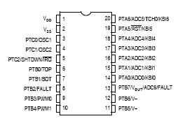
Pinout

  Connection Diagram


Specifications

Characteristic Symbol Value Unit
Supply voltage VDD 0.3 to +6.0 V
Input voltage VIN VSS0.3 to VDD +0.3
V
Maximum current per pin
excluding those specified below
I ±15 mA
Maximum current out of VSS IMVSS 100 mA
Maximum current into VDD IMVDD 100 mA
Storage temperature TSTG 55 to +150 °C


Customers Who Bought This Item Also Bought

Margin,quality,low-cost products with low minimum orders. Secure your online payments with SeekIC Buyer Protection.
Prototyping Products
DE1
Discrete Semiconductor Products
Crystals and Oscillators
Optical Inspection Equipment
Programmers, Development Systems
Audio Products
View more