MC68HC908GR16A

Features: For convenience, features have been organized to reflect:• Standard features• Features of the CPU081.2.1 Standard FeaturesFeatures include:• High-performance M68HC08 architecture optimized for C-compilers• Fully upward-compatible object code with M6805, M146805, a...

product image

MC68HC908GR16A Picture
SeekIC No. : 004416505 Detail

MC68HC908GR16A: Features: For convenience, features have been organized to reflect:• Standard features• Features of the CPU081.2.1 Standard FeaturesFeatures include:• High-performance M68HC08 arch...

floor Price/Ceiling Price

Part Number:
MC68HC908GR16A
Supply Ability:
5000

Price Break

  • Qty
  • 1~5000
  • Unit Price
  • Negotiable
  • Processing time
  • 15 Days
Total Cost: $ 0.00

SeekIC Buyer Protection PLUS - newly updated for 2013!

  • Escrow Protection.
  • Guaranteed refunds.
  • Secure payments.
  • Learn more >>

Month Sales

268 Transactions

Rating

evaluate  (4.8 stars)

Upload time: 2024/11/27

Payment Methods

All payment methods are secure and covered by SeekIC Buyer Protection PLUS.

Notice: When you place an order, your payment is made to SeekIC and not to your seller. SeekIC only pays the seller after confirming you have received your order. We will also never share your payment details with your seller.
Product Details

Description


Features:

For convenience, features have been organized to reflect:
• Standard features
• Features of the CPU08
1.2.1 Standard Features
Features include:
• High-performance M68HC08 architecture optimized for C-compilers
• Fully upward-compatible object code with M6805, M146805, and M68HC05 Families
• 8-MHz internal bus frequency
• Clock generation module supporting 1-MHz to 8-MHz crystals
• FLASH program memory security(1)
• On-chip programming firmware for use with host personal computer which does not require high voltage for entry
• In-system programming (ISP)
• System protection features:
Optional computer operating properly (COP) reset
Low-voltage detection with optional reset and selectable trip points for 3.3-V and 5.0-V operation
Illegal opcode detection with reset
Illegal address detection with reset
• Low-power design; fully static with stop and wait modes
• Standard low-power modes of operation:
Wait mode
Stop mode
• Master reset pin and power-on reset (POR)
• 16 Kbytes of on-chip FLASH memory
• 1 Kbyte of on-chip random-access memory (RAM)
• 406 bytes of FLASH programming routines read-only memory (ROM)
• Serial peripheral interface (SPI) module
• Enhanced serial communications interface (ESCI) module
• Fine adjust baud rate prescalers for precise control of baud rate
• Arbiter module:
Measurement of received bit timings for baud rate recovery without use of external timer
Bitwise arbitration for arbitrated UART communications
• LIN specific enhanced features:
Generation of LIN 1.2 break symbols without extra software steps on each message
Break detection filtering to prevent false interrupts
• Two 16-bit, 2-channel timer interface modules (TIM1 and TIM2) with selectable input capture,
output compare, and pulse-width modulation (PWM) capability on each channel
• Up to 8-channel, 10-bit successive approximation analog-to-digital converter (ADC) depending on
package choice
• BREAK (BRK) module to allow single breakpoint setting during in-circuit debugging
• Internal pullups on IRQ and RST to reduce customer system cost
• Up to 37 general-purpose input/output (I/O) pins, including:
28 shared-function I/O pins
Up to nine dedicated I/O pins, depending on package choice
• Selectable pullups on inputs only on ports A, C, and D. Selection is on an individual port bit basis.
During output mode, pullups are disengaged.
• High current 10-mA sink/source capability on all port pins
• Higher current 20-mA sink/source capability on PTC0PTC4
• Timebase module (TBM) with clock prescaler circuitry for eight user selectable periodic real-time
interrupts with optional active clock source during stop mode for periodic wakeup from stop using
an external crystal
• User selection of having the oscillator enabled or disabled during stop mode
• Up to 8-bit keyboard wakeup port depending on package choice
• 2 mA maximum current injection on all port pins to maintain input protection
• Available packages:
32-pin quad flat pack (LQFP)
48-pin quad flat pack (LQFP)
• Specific features of the MC68HC908GR16A in 32-pin LQFP are:
Port A is only 4 bits: PTA0PTA3; 4-pin keyboard interrupt (KBI) module
Port B is only 6 bits: PTB0PTB5; 6-channel ADC module
Port C is only 2 bits: PTC0PTC1
Port D is only 7 bits: PTD0PTD6; shared with SPI, TIM1, and TIM2 modules
Port E is only 2 bits: PTE0PTE1; shared with ESCI module
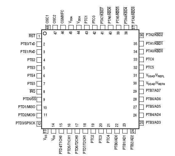
• Specific features of the MC68HC908GR16A in 48-pin LQFP are:
Port A is 8 bits: PTA0PTA7; 8-pin KBI module
Port B is 8 bits: PTB0PTB7; 8-channel ADC module
Port C is only 7 bits: PTC0PTC6
Port D is 8 bits: PTD0PTD7; shared with SPI, TIM1, and TIM2 modules
Port E is only 6 bits: PTE0PTE5; shared with ESCI module
1.2.2 Features of the CPU08
Features of the CPU08 include:
• Enhanced HC05 programming model
• Extensive loop control functions
• 16 addressing modes (eight more than the HC05)
• 16-bit index register and stack pointer
• Memory-to-memory data transfers
• Fast 8 * 8 multiply instruction
• Fast 16/8 divide instruction
• Binary-coded decimal (BCD) instructions
• Optimization for controller applications
• Efficient C language support


Pinout

  Connection Diagram


Specifications

Characteristic Symbol Value Unit
Supply voltage VDD 0.3 to +6.0 V
Input voltage
VIN VSS0.3 to VDD +0.3

V

Maximum current per pin excluding those specified below I ± 15 mA
Maximum current for pins PTC0PTC4 IPTC0PTC4 ± 25 mA
Maximum current out of VSS IMVSS 150 mA
Maximum current into VDD Imvdd 150 mA
Storage temperature TSTG 55 to +150 °C


Customers Who Bought This Item Also Bought

Margin,quality,low-cost products with low minimum orders. Secure your online payments with SeekIC Buyer Protection.
Batteries, Chargers, Holders
Cables, Wires - Management
Semiconductor Modules
Connectors, Interconnects
View more