MC68HC711PH8

Features: • Low power, high performance M68HC11 CPU core• 48K bytes of user ROM (MC68HC11PH8); 48K bytes of user EPROM (MC68HC711PH8)• 2K bytes of RAM• 768 bytes of byte-erasable user EEPROM, with on-chip charge pump• Up to 54 general purpose I/O lines, plus up to 8 i...

product image

MC68HC711PH8 Picture
SeekIC No. : 004416476 Detail

MC68HC711PH8: Features: • Low power, high performance M68HC11 CPU core• 48K bytes of user ROM (MC68HC11PH8); 48K bytes of user EPROM (MC68HC711PH8)• 2K bytes of RAM• 768 bytes of byte-eras...

floor Price/Ceiling Price

Part Number:
MC68HC711PH8
Supply Ability:
5000

Price Break

  • Qty
  • 1~5000
  • Unit Price
  • Negotiable
  • Processing time
  • 15 Days
Total Cost: $ 0.00

SeekIC Buyer Protection PLUS - newly updated for 2013!

  • Escrow Protection.
  • Guaranteed refunds.
  • Secure payments.
  • Learn more >>

Month Sales

268 Transactions

Rating

evaluate  (4.8 stars)

Upload time: 2024/11/27

Payment Methods

All payment methods are secure and covered by SeekIC Buyer Protection PLUS.

Notice: When you place an order, your payment is made to SeekIC and not to your seller. SeekIC only pays the seller after confirming you have received your order. We will also never share your payment details with your seller.
Product Details

Description


Features:

• Low power, high performance M68HC11 CPU core
• 48K bytes of user ROM (MC68HC11PH8); 48K bytes of user EPROM (MC68HC711PH8)
• 2K bytes of RAM
• 768 bytes of byte-erasable user EEPROM, with on-chip charge pump
• Up to 54 general purpose I/O lines, plus up to 8 input-only lines
• Non-multiplexed address and data buses, permitting direct access to the full 64K address map
• 16-bit timer with 3/4 input captures and 4/5 output compares; pulse accumulator and COP watchdog timer
• Three 8-bit modulus timers, for generating periodic interrupts
• Power saving PLL circuit
• Wired-OR interrupt capability for keyboard support, allowing wake-up from STOP and WAIT modes
• Two 8- or 9-bit SCI subsystems, one with MI BUS† capability; both NRZ type for RS232 compatibility
• Two SPI subsystems, with software selectable MSB/LSB first option
• 8-channel, 8-bit analog-to-digital (A/D) converter
• Four 8-bit PWM timer channels (may be concatenated to form one or two 16-bit channels)
• 4-segment LCD driver
• Available in 84-pin PLCC or 112-pin TQFP packages (MC68HC11PH8); also 84-pin CERQUAD package 68HC711PH8)


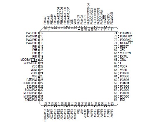
Pinout

  Connection Diagram


Specifications

Rating Symbol Value Value
Supply voltage (1) VDD Ð 0.3 to +7.0 V
Input voltage (1) VDD Ð 0.3 to +7.0 V
Operating temperature range
Ð MC68HC11PH8, MC68HC711PH8
Vin TL to TH
Ð40 to +85
°C
Storage temperature range Tstg Ð 55 to +150 °C
Current drain per pin (2)
Ð not VDD, VSS, VDD AD, VSS AD, VRH or VRL
ID 25 mA


(1) All voltages are with respect to VSS.
(2) Maximum current drain per pin is for one pin at a time, observing maximum power dissipation limits.

Note: This device contains circuitry designed to protect against damage due to high electrostatic voltages or electric fields. However, it is recommended that normal precautions be taken to avoid the application of any voltages higher than those given in the maximum ratings table to this high impedance circuit. For maximum reliability all unused inputs should be tied to either VSS or VDD.


Description

The central element of MC68HC711PH8 in the SPI system is the block containing the shift register and the read data buffer (see Figure 7-1). The system is single buffered in the transmit direction and double buffered in the receive direction. This means that new data for transmission cannot be written to the shifter until the previous transfer of MC68HC711PH8 is complete; however,  eceived data is transferred into a parallel read data buffer so the shifter is free to accept a second serial character. As long as the first character is read out of the read data buffer before the next serial character is ready to be transferred, no overrun condition occurs. A single MCU register address is used for reading data from the read data buffer and for writing data to the shifter.

The SPI MC68HC711PH8 status block represents the SPI status functions (transfer complete, write collision, and mode fault) performed by the serial peripheral status register (SPSR). The SPI MC68HC711PH8 control block represents those functions that control the SPI system through the serial peripheral control register (SPCR).


Customers Who Bought This Item Also Bought

Margin,quality,low-cost products with low minimum orders. Secure your online payments with SeekIC Buyer Protection.
LED Products
Resistors
Computers, Office - Components, Accessories
Audio Products
Tapes, Adhesives
803
Industrial Controls, Meters
View more