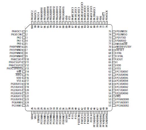
Features: • Low power, high performance M68HC11 CPU core with 4MHz internal bus frequency• 768 bytes of RAM• 640 bytes of byte-erasable EEPROM, with on-chip charge pump• 448 bytes of boot ROM• Up to 70 general purpose I/O lines, plus up to 10 input-only lines• N...
MC68HC11KW1: Features: • Low power, high performance M68HC11 CPU core with 4MHz internal bus frequency• 768 bytes of RAM• 640 bytes of byte-erasable EEPROM, with on-chip charge pump• 448 ...
SeekIC Buyer Protection PLUS - newly updated for 2013!
268 Transactions
All payment methods are secure and covered by SeekIC Buyer Protection PLUS.
• Low power, high performance M68HC11 CPU core with 4MHz internal bus frequency
• 768 bytes of RAM
• 640 bytes of byte-erasable EEPROM, with on-chip charge pump
• 448 bytes of boot ROM
• Up to 70 general purpose I/O lines, plus up to 10 input-only lines
• Non-multiplexed address and data buses, permitting direct access to the full 64K byte address map
• Memory expansion unit, with six address extension lines, allowing up to (for example) sixteen 32K byte banks of external memory to be addressed in either of two bank windows
• Four external chip selects
• 16-bit timer with 3/4 input captures and 5/4 output compares; pulse accumulator and COP watchdog timer
• Real-time interrupt circuit
• Two additional 16-bit timers, each with 3 output compares and one input capture or output compare (may be externally clocked, if required, for external event counter operation)
• SCI subsystem (NRZ type for compatibility with standard RS232 systems) with parity and a modulus prescaler
• SPI subsystem, with software selectable MSB/LSB first option and increased baud rate selection range
• 10-channel, 10-bit analog-to-digital converter
• Four 8-bit PWM timer channels
• Available in 100-pin TQFP package
Parameter |
Symbol |
Min |
Max |
Units |
Supply voltage (1) |
VDD |
-0.3 |
+7.0 |
V |
Input voltage (1) |
VIN |
-0.3 |
+7.0 |
V |
Operating temperature range |
TA |
TL |
TH +85 |
°C |
Storage temperature range |
TSTG |
-50 |
+150 |
°C |
Current drain per pin (2) not VDD,VSS,VDDAD,VSSAD,VRH,VRL or ports H, K, |
ID |
50 |
mA |
(1) All voltages are with respect to VSS.
(2) Maximum current drain per pin is for one pin at a time, observing maximum power dissipation limits.
Note: This device contains circuitry designed to protect against damage due to high electrostatic voltages or electric fields. However, it is recommended that normal precautions be taken to avoid the application of any voltages higher than those given in the maximum ratings table to this high impedance circuit. For maximum reliability all unused inputs should be tied to either VSS or VDD.