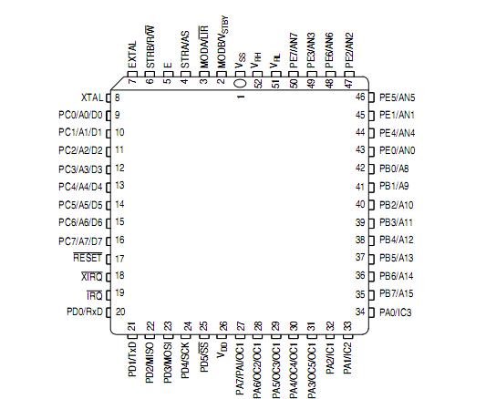
PinoutSpecifications Rating Symbol Value Unit Supply Voltage VDD 0.3 to + 7.0 V Input Voltage Vin 0.3 to + 7.0 V Operating Temperature RangeMC68HC11A8MC68HC11A8CMC68HC11A8VMC68HC11A8MMC68L11A8 TA TL to TH0 to 70 40 to 85 40 to 105 40 to 1...
MC68HC11A8: PinoutSpecifications Rating Symbol Value Unit Supply Voltage VDD 0.3 to + 7.0 V Input Voltage Vin 0.3 to + 7.0 V Operating Temperature RangeMC68...
SeekIC Buyer Protection PLUS - newly updated for 2013!
268 Transactions
All payment methods are secure and covered by SeekIC Buyer Protection PLUS.
Rating |
Symbol |
Value |
Unit |
Supply Voltage |
VDD |
0.3 to + 7.0 |
V |
Input Voltage |
Vin |
0.3 to + 7.0 |
V |
Operating Temperature Range MC68HC11A8 MC68HC11A8C MC68HC11A8V MC68HC11A8M MC68L11A8 |
TA |
TL to TH 0 to 70 40 to 85 40 to 105 40 to 125 20 to 70 |
°C |
Storage Temperature Range |
Tstg |
55 to 150 |
°C |
Current Drain per Pin* Excluding VDD, VSS, VRH, and VRL |
ID |
25 |
mA |
A block diagram of the SCI is shown in Figure 5-6. The user of MC68HC11A8 has option bits in serial communications control register 1 (SCCR1) to determine the "wake-up" method (WAKE bit) and data word length (M bit) of the SCI. Serial communications control reg- ister 2 (SCCR2) of MC68HC11A8 provides control bits which individually enable/disable the transmitter or receiver (TE and RE, respectively), enable system interrupts (TIE, TCIE, ILIE) and provide the wake-up enable bit (RWU) and the send break code bit (SBK). The baud rate register (BAUD) bits allow the user to select different baud rates which may be used as the rate control for the transmitter and receiver.
Data transmission is initiated by a write to the serial communications data register (SCDR). Provided the transmitter MC68HC11A8 is enabled, data stored in the SCDR MC68HC11A8 is transferred to the transmit data shift register. This transfer of data sets the TDRE bit of the SCI status registe(SCSR) and may generate an interrupt if the transmit interrupt is en- abled. The transfer of data to the transmit data shift register is synchronized with the bit rate clock (Figure 5-7). All data is transmitted LSB first. Upon completion of data transmission, the transmission complete (TC) bit of the SCSR is set (provided no pending data, preamble, or break is to be sent), and an interrupt may be generated if the transmit complete interrupt is enabled. If the transmitter MC68HC11A8 is disabled, and the data, preamble, or break (in the transmit shift register) has been sent, the TC bit will also be set. MC68HC11A8 will also generate an interrupt if the TCIE bit is set. If the transmitter is dis- abled in the middle of a transmission, that character will be completed before the trans- mitter gives up control of the TxD pin.