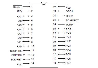
Features: • Low cost• HC05 core• 28-pin package• On-chip oscillator with RC (resistor capacitor) or crystal/ceramic resonator mask options• 4160 bytes of user read-only memory (ROM), including 16 user vector locations• ROM security feature(1)• 176 bytes of...
MC68HC05P4A: Features: • Low cost• HC05 core• 28-pin package• On-chip oscillator with RC (resistor capacitor) or crystal/ceramic resonator mask options• 4160 bytes of user read-only...
SeekIC Buyer Protection PLUS - newly updated for 2013!
268 Transactions
All payment methods are secure and covered by SeekIC Buyer Protection PLUS.
Deliver the application program to Motorola in one of the following media:
• Macintosh(1) 3 1/2-inch diskette (double-sided 800 K or double-sided high-density 1.4 M)
• MS-DOS(2) or PC-DOSTM(3) 3 1/2-inch diskette (double-sided
720 K or double-sided high-density 1.44 M)
• MS-DOS or PC-DOSTM 5 1/4-inch diskette (double-sided doubledensity 360 K or double-sided high-density 1.2 M)
Use positive logic for data and addresses.When submitting the application program on a diskette, clearly label the diskette with the following information:
• Customer name
• Customer part number
• Project or product name
• File name of object code
• Date
• Name of operating system that formatted diskette
• Formatted capacity of diskette
On diskettes, the application program must be in Motorola's S-record format (S1 and S9 records), a character-based object file format generated by M6805 cross assemblers and linkers.
NOTE: Begin the application program at the first user ROM location. Program addresses must correspond exactly to the available on-chip user ROM addresses as shown in the memory map. Write $00 in all non-user ROM locations or leave all non-user ROM locations blank. Refer to the current
Maximum ratings are the extreme limits to which the MCU can be exposed without permanently damaging it.
The MCU contains circuitry to protect the inputs against damage from high static voltages; however, do not apply voltages higher than those shown in the table here. Keep VIn and VOut within the range VSS (VIn or VOut) VDD. Connect unused inputs to the appropriate voltage level, either VSS or VDD
Rating |
Symbol |
Value |
Unit |
Supply voltage |
VDD |
0.3 to +7.0 |
V |
Input voltage |
VIn |
VSS 0.3 to VDD +0.3 |
V |
Self-check mode (IRQ pin only) |
VIn |
VSS 0.3 to 2 x VDD +0.3 |
V |
Current drain per pin excluding VDD and VSS |
I |
25 |
mA |
Storage temperature range |
TSTG |
65 to +150 |
°C |
Operating temperature range MC68HC05P4AP (standard) MC68HC05P4ACP (extended) |
TA |
TL to TH 0 to +70 40 to +85 |
°C |
Thermal resistance Plastic DIP Plastic SOIC |
JA |
60 71 |
°C/W |