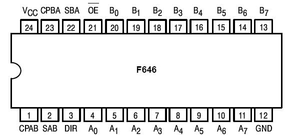
Features: • Independent Registers for A and B• Multiplexed Real-Time and Stored Data• Choice of True (F646) and Inverting (F648) Data Paths• 3-State OutputsPinoutDescriptionMC54FXXXJ consist of bus transceiver circuits with 3-state D-type flip-flops, and control circuitry a...
MC54FXXXJ: Features: • Independent Registers for A and B• Multiplexed Real-Time and Stored Data• Choice of True (F646) and Inverting (F648) Data Paths• 3-State OutputsPinoutDescriptionM...
SeekIC Buyer Protection PLUS - newly updated for 2013!
268 Transactions
All payment methods are secure and covered by SeekIC Buyer Protection PLUS.
PinoutDescriptionThe F373 contains eight D-type latches with 3-state output buffers. When the Latc...
PinoutDescriptionThe F374 consists of eight edge-triggered flip-flops with individual D-type input...
MC54FXXXJ consist of bus transceiver circuits with 3-state D-type flip-flops, and control circuitry arranged for multiplexed transmission of data directly from the input bus or from the internal registers. Data on the A or B bus will be clocked into the registers as the appropriate clock pin goes to a high logic level. Output Enable (OE) and DIR pins of MC54FXXXJ are provided to control the transceiver function. In the transceiver mode, data present at the high impedance port may be stored in either the A or the B register or in both. The select controls can multiplex stored and real-time (transparent mode) data.
The direction control of MC54FXXXJ determines which bus will receive data when the enable OE is Active LOW. In the isolation mode (OE HIGH), A data may be stored in the B register and/or B data may be stored in the A register.