MC34083

Features: • Wide Gain Bandwidth: 8.0 MHz for Fully Compensated DevicesWide Gain Bandwidth: 16 MHz for Decompensated Devices• High Slew Rate: 25 V/s for Fully Compensated Devices High Slew Rate: 50 V/s for Decompensated Devices• High Input Impedance: 1012• Input Offset Volta...

product image

MC34083 Picture
SeekIC No. : 004415892 Detail

MC34083: Features: • Wide Gain Bandwidth: 8.0 MHz for Fully Compensated DevicesWide Gain Bandwidth: 16 MHz for Decompensated Devices• High Slew Rate: 25 V/s for Fully Compensated Devices High Sle...

floor Price/Ceiling Price

Part Number:
MC34083
Supply Ability:
5000

Price Break

  • Qty
  • 1~5000
  • Unit Price
  • Negotiable
  • Processing time
  • 15 Days
Total Cost: $ 0.00

SeekIC Buyer Protection PLUS - newly updated for 2013!

  • Escrow Protection.
  • Guaranteed refunds.
  • Secure payments.
  • Learn more >>

Month Sales

268 Transactions

Rating

evaluate  (4.8 stars)

Upload time: 2024/11/27

Payment Methods

All payment methods are secure and covered by SeekIC Buyer Protection PLUS.

Notice: When you place an order, your payment is made to SeekIC and not to your seller. SeekIC only pays the seller after confirming you have received your order. We will also never share your payment details with your seller.
Product Details

Description


Features:

• Wide Gain Bandwidth: 8.0 MHz for Fully Compensated Devices
   Wide Gain Bandwidth: 16 MHz for Decompensated Devices
• High Slew Rate: 25 V/s for Fully Compensated Devices
   High Slew Rate: 50 V/s for Decompensated Devices
• High Input Impedance: 1012
• Input Offset Voltage: 0.5 mV Maximum (Single Amplifier)
• Large Output Voltage Swing: 14.7 V to +14 V for
   Large Output Voltage Swing: VCC/VEE = ±15 V
• Low Open Loop Output Impedance: 30 @ 1.0 MHz
• Low THD Distortion: 0.01%
• Excellent Phase/Gain Margins: 55°/7.6 dB for Fully Compensated Devices


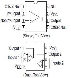
Pinout

  Connection Diagram


Specifications

Rating Symbol Value Unit
Supply Voltage (from VCC to VEE) VS +44 V
Input Differential Voltage Range VIDR (Note 1) V
Input Voltage Range VIR (Note 1) V
Output Short Circuit Duration (Note 2) tSC Indefinite sec
Operating Ambient Temperature Range TA 0 to +70 °C
Operating Junction Temperature TJ +125 °C
Storage Temperature Range Tstg 65 to +165 °C
NOTES:
1. Either or both input voltages must not exceed the magnitude of VCC or VEE.
2. Power dissipation must be considered to ensure maximum junction temperature (TJ) is not exceeded.


Description

MC34083 is a new generation of high speed JFET input monolithic operational amplifiers. Innovative design concepts along with JFET technology provide wide gain bandwidth product and high slew rate. Wellmatched JFET input MC34083 and advanced trim techniques ensure low input offset errors and bias currents. The all NPN output stage features large output voltage swing, no deadband crossover distortion, high capacitive drive capability, excellent phase and gain margins, low open loop output impedance, and symmetrical source/sink AC frequency response.

MC34083 is available in fully compensated or decompensated (AVCL2) and is specified over a commercial temperature range. MC34083 is pin compatible with existing Industry standard operational amplifiers, and allow the designer to easily upgrade the performance of existing designs.


Customers Who Bought This Item Also Bought

Margin,quality,low-cost products with low minimum orders. Secure your online payments with SeekIC Buyer Protection.
Fans, Thermal Management
Prototyping Products
DE1
Discrete Semiconductor Products
Cables, Wires
RF and RFID
Soldering, Desoldering, Rework Products
View more