MC34071,2,4A

Features: • Wide Bandwidth: 4.5 MHz• High Slew Rate: 13 V/s• Fast Settling Time: 1.1 ms to 0.1%• Wide Single Supply Operation: 3.0 V to 44 V• Wide Input Common Mode Voltage Range: Includes Ground (VEE)• Low Input Offset Voltage: 3.0 mV Maximum (A Suffix)• ...

product image

MC34071,2,4A Picture
SeekIC No. : 004415884 Detail

MC34071,2,4A: Features: • Wide Bandwidth: 4.5 MHz• High Slew Rate: 13 V/s• Fast Settling Time: 1.1 ms to 0.1%• Wide Single Supply Operation: 3.0 V to 44 V• Wide Input Common Mode Vol...

floor Price/Ceiling Price

Part Number:
MC34071,2,4A
Supply Ability:
5000

Price Break

  • Qty
  • 1~5000
  • Unit Price
  • Negotiable
  • Processing time
  • 15 Days
Total Cost: $ 0.00

SeekIC Buyer Protection PLUS - newly updated for 2013!

  • Escrow Protection.
  • Guaranteed refunds.
  • Secure payments.
  • Learn more >>

Month Sales

268 Transactions

Rating

evaluate  (4.8 stars)

Upload time: 2024/11/27

Payment Methods

All payment methods are secure and covered by SeekIC Buyer Protection PLUS.

Notice: When you place an order, your payment is made to SeekIC and not to your seller. SeekIC only pays the seller after confirming you have received your order. We will also never share your payment details with your seller.
Product Details

Description


Features:

• Wide Bandwidth: 4.5 MHz
• High Slew Rate: 13 V/s
• Fast Settling Time: 1.1 ms to 0.1%
• Wide Single Supply Operation: 3.0 V to 44 V
• Wide Input Common Mode Voltage Range: Includes Ground (VEE)
• Low Input Offset Voltage: 3.0 mV Maximum (A Suffix)
• Large Output Voltage Swing: 14.7 V to +14 V (with ±15 V Supplies)
• Large Capacitance Drive Capability: 0 pF to 10,000 pF
• Low Total Harmonic Distortion: 0.02%
• Excellent Phase Margin: 60°
• Excellent Gain Margin: 12 dB
• Output Short Circuit Protection
• ESD Diodes/Clamps Provide Input Protection for Dual and Quad


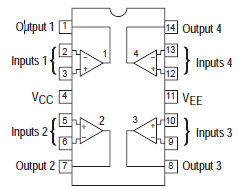
Pinout

  Connection Diagram


Specifications

Rating
Symbol
Value
Unit
Supply Voltage (VCC to VEE)
VS
+36
V
Input Differential Voltage Range
VIDR
(Note 1)
V
Input Voltage Range
VIR
(Note 1)
V
Output Short Circuit Duration (Note 2)
tSC
Indefinite
sec
Operating Junction Temperature
TJ
+150
Storage Temperature
Tstg
60 to +150
NOTES: 1. Either or both input voltages should not exceed the magnitude of VCC or VEE.
            2. Power dissipation must be considered to ensure maximum junction temperature (TJ) is not exceeded (see Figure 1).


Description

Quality bipolar fabrication with innovative design concepts are employed for the MC33071/72/74, MC34071/72/74 series of monolithic operational amplifiers. MC33071/72/74, MC34071/72/74 series of operational amplifiers offer 4.5 MHz of gain bandwidth product, 13 V/ms slew rate and fast setting time without the use of JFET device technology. Although this series can be operated from split supplies, MC33071/72/74, MC34071/72/74 series is particularly suited for single supply operation, since the common mode input voltage range includes ground potential (VEE). With A Darlington input stage, this series exhibits high input resistance, low input offset voltage and high gain. The all NPN output stage, characterized by no deadband crossover distortion and large output voltage swing, provides high capacitance drive capability, excellent phase and gain margins, low open loop high frequency output impedance and symmetrical source/sink AC frequency response.

The MC33071/72/74, MC34071/72/74 series of devices are available in standard or prime performance (A Suffix) grades and are specified over the commercial, industrial/vehicular or military temperature ranges. The MC33071/72/74, MC34071/72/74 series series of single, dual and quad operational amplifiers are available in plastic DIP, SOIC and TSSOP surface mount packages.


Customers Who Bought This Item Also Bought

Margin,quality,low-cost products with low minimum orders. Secure your online payments with SeekIC Buyer Protection.
Semiconductor Modules
Fans, Thermal Management
Transformers
Tapes, Adhesives
803
RF and RFID
View more