Features: ·VDD1: 5.0 V low drop voltage regulator, current limitation, overtemperature detection, monitoring and reset function with total current capability 200 mA
·V2: tracking function of VDD1 regulator; control circuitry for external bipolar ballast transistor for high flexibility in hoice of peripheral voltage and current supply
·Four operational modes
·Low standby current consumption in Stop and Sleep modes
·Built-in low speed 125 kbps fault tolerant CAN physical interface.
·External high voltage wake-up input, associated with HS1 VBAT switch
·150 mA output current capability for HS1 VBAT switch allowing drive of external switches pull-up resistors or relays
·Pb-Free Packaging Designated by Suffix Code EG
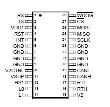
Pinout Specifications
| Ratings |
Symbol |
Max |
Unit |
| ELECTRICAL RATINGS |
Supply Voltage at VSUP
Continuous voltage
Transient voltage (Load dump) |
VSUP |
-0.3 to 27
40 |
V |
Logic Signals
(RX, TX, MOSI, MISO, CS, SCLK, RST, WDOG, INT) |
VLOG |
-0.3 to VDD1 +0.3 |
V |
| Output current VDD1 |
I |
Internally Limited |
mA |
HS1
Voltage
Output Current |
V
I |
-0.2 to VSUP +0.3
Internally Limited |
V
A |
L0, L1
DC Input voltage
DC Input current
Transient input voltage (according to ISO7637 specification) and with external component per Figure 3. |
VWU
IWU
VTRWU |
-0.3 to 40
-2.0 to 2.0
+-100 |
V
mA
V |
| DC voltage at V2 (V2INT) |
V2INT |
0 to 5.25 |
V |
| DC Voltage On Pins CANH, CANL |
VBUS |
-20 to +27 |
V |
Transient Voltage At Pins CANH, CANL
0.0 < V2-INT < 5.5 V; VSUP = 0.0; T < 500 ms |
VCANH/VCANL |
-40 to +40 |
V |
Transient Voltage On Pins CANH, CANL
(Coupled Through 1.0 nF Capacitor) |
VTR |
-150 to +100 |
V |
| DC Voltage On Pins RTH, RTL |
VRTL, VRTH |
-0.3 to +27V |
V |
Transient Voltage At Pins RTH, RTL
0.0 < V2-INT < 5.5 V; VSUP = 0.0; T < 500 ms |
VRTH/VRTL |
-0.3 to +40 |
V |
DescriptionAn SBC device is a monolithic IC combining many functions repeatedly found in standard microcontroller-based systems, e.g., protection, diagnostics, communication, power, etc. The 33889 is an SBC having fully protected, fixed 5.0 V low drop-out regulator, with current limit, over-temperature pre-warning and reset.
An output drive with sense input of 33889 is also provided to implement a second 5.0 V regulator using an external PNP. The 33889 has Normal, Standby, Stop and Sleep modes; an internally switched high-side power supply output with two wake-up inputs; programmable timeout or window watchdog, Interrupt, Reset, SPI input control, and a low-speed fault tolerant CAN transceiver, compatible with CAN 2.0 A and B protocols for module-to-module communications. The combination of 33889 is an economical solution for power management, high-speed communication, and control in MCU-based systems.

 MC33889BDW/R2 Data Sheet


