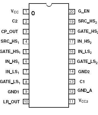
Features: • VCC Operating Voltage Range from 5.5 V up to 55 V• VCC2 Operating Voltage Range from 5.5 V up to 28 V• Automotive Temperature Range -40°C to 125°C• 1A Pulse Current Output Driver• Fast PWM Capability• Built-In Charge PumpPinoutSpecifications Rat...
MC33883: Features: • VCC Operating Voltage Range from 5.5 V up to 55 V• VCC2 Operating Voltage Range from 5.5 V up to 28 V• Automotive Temperature Range -40°C to 125°C• 1A Pulse Curre...
SeekIC Buyer Protection PLUS - newly updated for 2013!
268 Transactions
All payment methods are secure and covered by SeekIC Buyer Protection PLUS.
Ratings | Symbol | Min | Max | Unit |
Supply Voltage1 Supply Voltage2 (NOTE 1) Linear Regulator Output Voltage High Side Floating Supply Absolute Voltage High Side Floating Source Voltage High Side Source Current from Cpout in Switch On State |
VCC VCC2 VLR_out VCP_OUT VSRC_HS IS |
-0.3 -0.3 -0.3 -0.3 -0.3 |
65 35 18 65 65 250 |
V V V V V mA |
High Side Gate Voltage High Side Gate Source Voltage High Side Floating Supply Gate Voltage Low Side Output Voltage Wake up Voltage Logic Input Voltage Charge Pump Capacitor Voltage Charge Pump Capacitor Voltage |
VGATE_HS VGATE_HS - VSRC_HS VCP_OUT - VGATE_HS VGATE_LS VG_EN VIN VC1 VC2 |
-0.3 -0.3 -0.3 -0.3 -0.3 -0.3 -0.3 -0.3 -0.3 |
65 20 65 17 17 35 10 VLR_OUT 65 |
V V V V V V V V |
ESD Voltage on all Pins except the case of (Pin C2 respect to PinVcc) (HBM, 100pF, 1.5kOhms) ESD Voltage (PinC2 respect to Pin Vcc) Power Dissipation and Thermal Characteristics Maximum Power Dissipation@25°C Thermal Resistance Junction-to-Air Operating Junction Temperature Storage Temperature |
VESD VESD2 PD RJA TJ Tstg |
-2.0 -1.7 -40 -65 |
2.0 1.7 1.25 100 +150 +150 |
KV KV W °C/W °C °C |
The MC33883 is a full bridge pre-driver including integrated charge pump, two independent high and low side driver channels.
The drive outputs of MC33883 are capable to source and sink 1 A pulse peak current. The low side channel is referenced to ground, the high side channel is floating above ground.
A linear regulator of MC33883 provides a maximum of 16.5V to supply the low side gate driver stages. The high side driver stages are supplied with a 10Vtypical charge pump voltage. Such built-in feature, associated to external capacitor provides a full floating high side drive.
An under- and over-voltage protection prevents erratic system operation at abnormal supply voltages. Under fault, these functions of MC33883 force the driver stages into off state. The logic inputs are compatible with standard CMOS or LSTTL outputs. The input hysteresis makes the output switching time independent of the input transition time.
The global enable logic signal can be used to disable the charge pump and all the bias circuit. The net advantage of MC33883 is the reduction of the quiescent supply current to under 10µA. To wake up the circuit, 5 V has to be provided at G_EN.