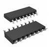
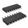
DescriptionThe MC33596A belongs to MC33596 family which is a highly integrated receiver designed for low-voltage applications. A configuration switching feature allows automatic changing of the configuration between two programmable settings without the need of an MCU. MC33596A includes a programmable PLL for multi-channel applications, an RSSI circuit, a strobe oscillator that periodically wakes up the receiver while a data manager checks the content of incoming messages.
The features of MC33596A can be summarized as (1)304 MHz, 315 MHZ, 426 MHZ, 434 MHZ, 868 MHZ, and 915 MHz ISM bands; (2)choice of temperature ranges: - 40°C to +85°C - 20°C to +85°C; (3)OOK and FSK reception; (4)20 kbps maximum data rate using manchester coding; (5)2.1 V to 3.6 V or 5 V supply voltage; (6)Programmable via SPI; (7)6 kHz PLL frequency step; (8)current consumption: - 10.3 mA in RX mode - less then 1 mA in RX mode with strobe ratio = 1/10 - 260 nA standby and 24 A off currents; (9)configuration switching - allows fast switching of two register banks.
The absolute maximum ratings of MC33596A are (1)supply voltage on pin: VCCIN VCCIN VGND: 0.3 to 5.5 V; (2)supply voltage on pins: VCCINOUT, VCCDIG VCC VGND: 0.3 to 3.6 V; (3)Supply voltage on pins: VCC2IN, VCC2RF, VCC2VCO VCC2 VGND: 0.3 to 2.7 V; (4)voltage allowed on each pin (except digital pins) - VGND: 0.3 to VCC2 V; (5)voltage allowed on digital pins: SEB, SCLK, MISO, MOSI, CONFB, DATACLK, RSSIC, STROBE VCCIO VGND: 0.3 to VCCIN+0.3 V; (6)ESD HBM voltage capability on each pin1: ±2000 V; (7)ESD MM voltage capability on each pin2: ±200 V; (8)solder heat resistance test (10 s): 260 °C; (9)storage temperature TS: 65 to +150 °C; (10)junction temperature TJ: 150 °C.

 MC33596A Data Sheet


