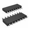
DescriptionThe MC33567D-2 is designed as dual linear power supply controller which is designed to facilitate power management for motherboard applications where reliable regulation of high current supply planes is required. MC33567D-2 provides the drive, sense and control signals to interface two ...
MC33567D-2: DescriptionThe MC33567D-2 is designed as dual linear power supply controller which is designed to facilitate power management for motherboard applications where reliable regulation of high current s...
SeekIC Buyer Protection PLUS - newly updated for 2013!
268 Transactions
All payment methods are secure and covered by SeekIC Buyer Protection PLUS.
The MC33567D-2 is designed as dual linear power supply controller which is designed to facilitate power management for motherboard applications where reliable regulation of high current supply planes is required. MC33567D-2 provides the drive, sense and control signals to interface two external, N−channel MOSFETs for regulating two different supply planes. Undervoltage short circuit detection places the operation of the system into a protected mode pending removal of the short.
MC33567D-2 has seven features. (1)Two independent regulated supplies. (2)Undervoltage short circuit protection. (3)Supply undervoltage detection. (4)Drive capability for N-channel MOSFETs. (5)Bypass function for 3.3V AGP card detection. (6)Pb-free package may be available. The G−Suffix denotes a Pb-free lead finish. (7)Dual 2.525V supplies for clock and memory. Those are all the main features.
Some absolute maximum ratings of MC33567D-2 have been concluded into several points as follow. (1)supply voltage would be 12.5V. (2)Its shutdown voltage would be Vcc. (3)Its operating ambient temperature range would be from 0°C to 80°C. (4)Its operating junction temperature range would be from -50°C to 125°C. (5)Its lead temperature soldering 10 seconds would be 300°C. (6)Its storage temperature range would be from -55°C to 150°C. (7)Its package thermal resistance, junction to ambient would be 159°C/W. (8)Its thermal resistance junction to case would be 28°C/W. It should be noted that stresses above those listed in absolute maximum ratings may cause permanent damage to device.
Also some electrical characteristics of MC33567D-2 are concluded as follow. (1)Its supply voltage would be min 9.0V and typ 12V and max 12.5V. (2)Its quiescent current would be typ 5.8mA and max 9.0A at Vshdn1=Vshdn2=0V. (3)Its undervoltage lockout threshold voltage (Vcc increasing) would be min 7.0V and typ 8.5V and max 9.0V. (4)Its hysteresis voltage (Vcc decreasing) would be min 0.2V and typ 0.5V and max 0.9V. And so on. If you have any question or suggestion or want to know more information about MC33567D-2 please contact us for details. Thank you!