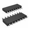
DescriptionThe MC33385DH is designed as a quad low side driver fully protected switch. This device is a general purpose low side driver but has been especially designed to operate in engine management application as injector driver or automotive gear box. MC33385DH is interfaced directly with a mi...
MC33385DH: DescriptionThe MC33385DH is designed as a quad low side driver fully protected switch. This device is a general purpose low side driver but has been especially designed to operate in engine manageme...
SeekIC Buyer Protection PLUS - newly updated for 2013!
268 Transactions
All payment methods are secure and covered by SeekIC Buyer Protection PLUS.
The MC33385DH is designed as a quad low side driver fully protected switch. This device is a general purpose low side driver but has been especially designed to operate in engine management application as injector driver or automotive gear box. MC33385DH is interfaced directly with a microcontroller for parallel control of the load and the individual output diagnostic is done through a SPI.
MC33385DH has nine features. (1)RDSON of 250mW per output at 25°C. (2)Supplied from the main 5V Vcc. (3)Input CMOS compatible. (4)Diagnostic through SPI. (5)Nominal current of 2A per output. (6)Current limitation at 3A with automatic turn off. (7)Output internally clamped at 50V typ for inductive load drive. (8)Junction to case thermal resistance of 4.4°C/W. (9)Individual output over temperature shutdown. Those are all the main features.
Some absolute maximum ratings of MC33385DH have been concluded into several points as follow. (1)Its voltage range would be from -0.3V to 7V. (2)Its continuous output voltage (with no reverse current) would be from -0.3V to 45V. (3)Its continuous current would be max 2.5A. (4)Its peak output current would be from -10A to Iscbmax. (5)Its clamped energy at the switching OFF would be max 70mJ for 1ms. (6)Its input voltage (inputs) would be from -0.3V to Vcc+0.3V. (7)Its input protection diode current would be min -20mA and max 1mA. (8)Its input voltage (outputs) would be from -0.3V to Vcc+0.3V. (9)Its input protection diode current for output SDO would be min -20mA and max 1mA. (10)Its operating junction temperature range would be from -40°C to 150°C. (11)Its thermal resistance junction to case would be max 4.5K/W. (12)Its thermal resistance junction to ambient would be max 50K/W. It should be noted that stresses above those listed in absolute maximum ratings may cause permanent damage to device.
Also some electrical characteristics of MC33385DH are concluded as follow. (1)Its standby current without load would be max 7mA. (2)Its operating mode would be max 17mA. (3)Its low threshold would be min -0.3V and max 0.2Vcc. (4)Its high threhold would be min 0.7Vcc and max Vcc+0.3. And so on. If you have any question or suggestion or want to know more information about MC33385DH please contact us for details. Thank you!