Features: • 1V platform compatible: ON voltage = 900mV, OFF voltage = 300mV max• Priority management system prevents power modulation before negative bias establishes• High performance 4.5MHz gainbandwidth product operational amplifier• Drives N or Pchannel MOSFET• 2....
MC33170: Features: • 1V platform compatible: ON voltage = 900mV, OFF voltage = 300mV max• Priority management system prevents power modulation before negative bias establishes• High perform...
SeekIC Buyer Protection PLUS - newly updated for 2013!
268 Transactions
All payment methods are secure and covered by SeekIC Buyer Protection PLUS.
• 1V platform compatible: ON voltage = 900mV, OFF voltage = 300mV max
• Priority management system prevents power modulation before negative bias establishes
• High performance 4.5MHz gainbandwidth product operational amplifier
• Drives N or Pchannel MOSFET
• 2.5V lownoise LDO
• Idle mode input for very low power consumption (standby mode)
Rating |
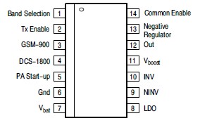
Pin NO. |
Symbol |
Value MIN |
Value MAX |
Units |
Band selection |
1 |
Vband |
0 |
5.5 |
V |
Tx Enable |
2 |
TxEn |
0 |
5.5 |
V |
GSM-900 |
3 |
VGSM |
-5 |
5.5 |
V |
DCS-1800 |
4 |
VDCS |
-5 |
5.5 |
V |
PA Start-up |
5 |
Vstartup |
0 |
5.5 |
V |
Vbat |
7 |
Vbat |
0 |
5.5 |
V |
NINY |
9 |
V+ |
0 |
5.5 |
V |
INY |
10 |
V- |
0 |
5.5 |
V |
Boost voltage |
11 |
Vboost |
0 |
5.5 |
V |
Negative regulation pin |
13 |
VZ |
-5.4 |
5.5 |
V |
Common Enable |
14 |
CE |
0 |
5.5 |
V |
ESD capability,HBM model |
AII pins |
2 |
kV | ||
ESD capability,Machine mondel |
AII pins |
200 |
V | ||
Steering Switch,continuous ouytput current Steering Switch,continuous ouytput cuttrnt Steering Switch,prak output current<1s |
3-4 5 5 |
GSM/DCS PA startup PA startup |
1 50 700 |
mA mA mA | |
Maximum power dissipation NW suffix,plastic packagr @Tj=25 NW suffix,plastic packagr @Tj=85 Thermal resistance Junction-to-Air |
PD PD RJ-A |
500 200 200 |
mW | ||
Operating Ambient Temperature Maximum Junction Temperature Maximum Operating Junction Temperature |
TA Tjmax Tj |
-40 to +85 150 125 |
| ||
Storage Temperature Range |
TSTG |
-60 to +150 |
Note1: The control pins, CE, TxEn and Bands shall never exceed Vcc + 0.3V
Note2: A 100nF decoupling capacitor is recommended between the IC Vcc and ground
Note3: To avoid any damage to the IC, the following sequence must be secured: CE goes up then Tx goes up > modulation startup TX goes down then CE goes down > modulation stop
The MC33170 is a complete solution for drain modulated dualband GSM 900MHz and DCS1800MHz Power Amplifiers.
Thanks to its internal decoder, the MC33170 drastically simplifies the interface between the PAs and the baseband logic section, providing an immediate gain in part count but also in occupied copper area. The MC33170 is also ready for 1V platforms since it accepts logic high control signals down to 900mV@25.
A priority management system of MC33170 ensures the negative is present before authorizing the power modulation, giving the necessary ruggedness to the final design. This function can easily be disabled for PAs not requiring a negative bias.
The MC33170 is able to directly drive an external P or Nchannel with the possibility to linearize the overall response via the internal highperformance control amplifier and easily implement system gain.
Finally, an LDO delivers a stable voltage, usable for external biasing purposes.