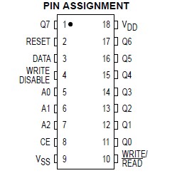
Features: The MC14099B and MC14599B are 8bit addressable latches. Data is entered in serial form when the appropriate latch is addressed (via address pins A0, A1, A2) and write disable is in the low state. Chip enable must be high for writing into MC14599B. For the MC14599B the data pin is a bidir...
MC14599B: Features: The MC14099B and MC14599B are 8bit addressable latches. Data is entered in serial form when the appropriate latch is addressed (via address pins A0, A1, A2) and write disable is in the low...
SeekIC Buyer Protection PLUS - newly updated for 2013!
268 Transactions
All payment methods are secure and covered by SeekIC Buyer Protection PLUS.
The MC14099B and MC14599B are 8bit addressable latches. Data is entered in serial form when the appropriate latch is addressed (via address pins A0, A1, A2) and write disable is in the low state. Chip enable must be high for writing into MC14599B. For the MC14599B the data pin is a bidirectional data port and for the MC14099B the input is a unidirectional write only port. The Write/Read line controls this port in the MC14599B.
The data is presented in parallel at the output of the eight latches independently of the state of Write Disable, rite/Read or Chip Enable.
A Master Reset capability is available on both parts.
• Serial Data Input
• Parallel Output
• Master Reset
• Supply Voltage Range = 3.0 Vdc to 18 Vdc
• Capable of Driving Two Lowpower TTL Loads or One LowPower Schottky TTL
Load over the Rated Temperature Range
• MC14099B pin for pin compatible with CD4099B
The MC14099B and MC14599B are 8bit addressable latches. Data is entered in serial form when the appropriate atch is addressed (via address pins A0, A1, A2) and write disable is in the low state. Chip enable must be high for writing into MC14599B. For the MC14599B the data pin is a bidirectional data port and for the MC14099B the input is a unidirectional write only port. The Write/Read line controls this port in the MC14599B.
The data is presented in parallel at the output of the eight latches independently of the state of Write Disable, Write/Read or Chip Enable.
A Master Reset capability is available on both parts.
• Serial Data Input
• Parallel Output
• Master Reset
• Supply Voltage Range = 3.0 Vdc to 18 Vdc
• Capable of Driving Two Lowpower TTL Loads or One LowPower Schottky TTL Load over the Rated
Temperature Range
• MC14099B pin for pin compatible with CD4099B
Symbol | Parameter | Value | Unit |
VDD | DC Supply Voltage | 0.5 to + 18.0 | V |
Vin, Vout | Input or Output Voltage (DC or Transient) | 0.5 to VDD + 0.5 | V |
Iin, Iout | Input or Output Current (DC or Transient), per Pin |
± 10 | mA |
PD | Power Dissipation, per Package† | 500 | mw |
Tstg | Storage Temperature | 65 to + 150 |
°C |
TL | Lead Temperature (8Second Soldering) |
°C |