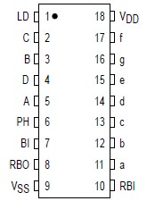
Pinout Specifications
|
Rating |
Symbol |
Value |
Unit |
|
DC Supply Voltage |
VDD |
0.5 to + 18 |
V |
|
Input Voltage, All Inputs |
Vin |
0.5 to VDD + 0.5 |
V |
|
DC Input Current per Pin |
Iin |
± 10 |
mAdc |
|
Operating Temperature Range |
TA |
55 to + 125 |
°C |
|
Power Dissipation, per Package† |
PD |
500 |
mW |
|
Storage Temperature Range |
Tstg |
65 to + 150 |
°C |
|
Maximum Continuous Output Drive
Current (Source or Sink) per Output |
IOHmax
IOLmax |
10 |
mAdc |
|
Maximum Continuous Output Power*
(Source or Sink) per Output |
POHmax
POLmax |
70 |
mW |
* POHmax = IOH (VOH VDD) and POLmax = IOL (VOL VSS)
* Maximum Ratings are those values beyond which damage to the device may occur.
†Temperature Derating: Plastic "P and D/DW" Packages: 7.0 mW/°C From 65°C To 125�C Ceramic "L" Packages: 12 mW/°C From 100°C To 125°C
DescriptionThe MC14544B BCDtoseven segment latch/decoder/driver is designed for use with liquid crystal readouts, and is constructed with complementary MOS (CMOS) enhancement mode devices. The circuit provides the functions of a 4bit storage latch and an 8421 BCDtoseven segment decoder and driver. The MC14544B has the capability to invert the logic levels of the output combination. The phase (Ph), blanking (BI), and latch disable (LD) inputs are used to reverse the truth table phase, blank the display, and store a BCD code, respectively. For liquid crystal (LC) readouts, a square wave is applied to the Ph input of the circuit and the electrically common backplane of the display. The outputs of the MC14544B are connected directly to the segments of the LC readout. The Ripple Blanking Input (RBI) and the Ripple Blanking Output (RBO) can be used to suppress either leading or trailing zeroes.
For other types of readouts, such as lightemitting diode (LED), incandescent, gas discharge, and fluorescent readouts, connection diagrams are given on this data sheet.
Applications of MC14544B include instrument (e.g., counter, DVM etc.) display driver, computer/calculator display driver, cockpit display driver, and various clock, watch, and timer uses.
• Latch Storage of Code
• Blanking Input
• Readout Blanking on All Illegal Input Combinations
• Direct LED (Common Anode or Cathode) Driving Capability
• Supply Voltage Range = 3.0 V to 18 V
• Capability for Suppression of Nonsignificant zero
• Capable of Driving Two Lowpower TTL Loads, One Lowpower Schottky TTL Load or Two HTL Loads Over the Rated Temperature Range

 MC14544B Data Sheet


