MC1451582

Features: • Operating Temperature Range: 40 to 85°C• Low Power Consumption Through Use of CMOS Technology• 3.0 to 9.0 V Supply Range• On or OffChip Reference Oscillator Operation• Lock Detect Signal• ÷ N Counter Output Available• Single Modulus/Parallel P...

product image

MC1451582 Picture
SeekIC No. : 004415392 Detail

MC1451582: Features: • Operating Temperature Range: 40 to 85°C• Low Power Consumption Through Use of CMOS Technology• 3.0 to 9.0 V Supply Range• On or OffChip Reference Oscillator Oper...

floor Price/Ceiling Price

Part Number:
MC1451582
Supply Ability:
5000

Price Break

  • Qty
  • 1~5000
  • Unit Price
  • Negotiable
  • Processing time
  • 15 Days
Total Cost: $ 0.00

SeekIC Buyer Protection PLUS - newly updated for 2013!

  • Escrow Protection.
  • Guaranteed refunds.
  • Secure payments.
  • Learn more >>

Month Sales

268 Transactions

Rating

evaluate  (4.8 stars)

Upload time: 2024/11/27

Payment Methods

All payment methods are secure and covered by SeekIC Buyer Protection PLUS.

Notice: When you place an order, your payment is made to SeekIC and not to your seller. SeekIC only pays the seller after confirming you have received your order. We will also never share your payment details with your seller.
Product Details

Description


Features:

• Operating Temperature Range: 40 to 85°C
• Low Power Consumption Through Use of CMOS Technology
• 3.0 to 9.0 V Supply Range
• On or OffChip Reference Oscillator Operation
• Lock Detect Signal
• ÷ N Counter Output Available
• Single Modulus/Parallel Programming
• 8 UserSelectable ÷ R Values: 8, 128, 256, 512, 1024, 2048, 2410, 8192
• ÷ N Range = 3 to 16383
• "Linearized" Digital Phase Detector Enhances Transfer Function Linearity
• Two Error Signal Options: SingleEnded (ThreeState) or DoubleEnded
• Chip Complexity: 8000 FETs or 2000 Equivalent Gates


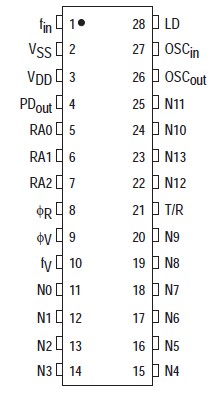
Pinout

  Connection Diagram


Specifications

Symbol

Parameter

Value

Unit

VDD

DC Supply Voltage

0.5 to + 10.0

V

Vin, Vout

Input or Output Voltage (DC or Transient) except SW1, SW2

0.5 to VDD + 0.5

V

Vout

Output Voltage (DC or Transient),
SW1, SW2 (Rpullup = 4.7 kW)

0.5 to + 15

V

Iin, Iout

Input or Output Current (DC or Transient), per Pin

± 10

mA

IDD, ISS

Supply Current, VDD or VSS Pins

± 30

mA

PD

Power Dissipation, per Package†

500

mW

Tstg

Storage Temperature

65 to + 150

°C

TL

Lead Temperature, 1 mm from Case for 10 seconds

260

°C


Description

MC1451582 contain protection circuitry to protect against damage due to high static voltages or electric fields. However, precautions must be taken to avoid applications of any voltage higher than maximum rated voltages to these highimpedance circuits. For proper operation, Vin and Vout should be constrained to the range VSS (Vin or Vout)  VDD except for SW1 and SW2.

SW1 and SW2 can be tied through external resistors to voltages as high as 15 V, independent of the supply voltage.

Unused inputs of MC1451582 must always be tied to an appropriate logic voltage level (e.g., either VSS or VDD), except for inputs with pullup devices. Unused outputs must be left open.


Customers Who Bought This Item Also Bought

Margin,quality,low-cost products with low minimum orders. Secure your online payments with SeekIC Buyer Protection.
Cable Assemblies
Test Equipment
Connectors, Interconnects
RF and RFID
Audio Products
View more