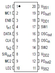
PinoutSpecifications Symbol Rating Value Unit VDD DC Supply Voltage 0.5 to + 10 V Vin, Vout Input or Output Voltage (DC or Transient)except SW1, SW2 0.5 to VDD + 0.5 V Vout Output Voltage (DC or Transient) - SW1,SW2 0.5 to 15 V Iin,...
MC145149: PinoutSpecifications Symbol Rating Value Unit VDD DC Supply Voltage 0.5 to + 10 V Vin, Vout Input or Output Voltage (DC or Transient)except SW1, SW2 0.5 to...
SeekIC Buyer Protection PLUS - newly updated for 2013!
268 Transactions
All payment methods are secure and covered by SeekIC Buyer Protection PLUS.
Symbol |
Rating |
Value |
Unit |
VDD |
DC Supply Voltage |
0.5 to + 10 |
V |
Vin, Vout |
Input or Output Voltage (DC or Transient) except SW1, SW2 |
0.5 to VDD + 0.5 |
V |
Vout |
Output Voltage (DC or Transient) - SW1, SW2 |
0.5 to 15 |
V |
Iin, Iout |
Input or Output Current (DC or Transient), per Pin |
± 10 |
mA |
IDD, ISS |
Supply Current, VDD or VSS Pins |
± 30 |
mA |
PD |
Power Dissipation, per Package† |
500 |
mW |
Tstg |
Storage Temperature |
65 to + 150 |
°C |
TL |
Lead Temperature (8Second Soldering) |
600 |
°C |
* Maximum Ratings are those values beyond which damage to the device may occur.
†Power Dissipation Temperature Derating: Plastic DIP: 12 mW/°C from 65 to 85°C SOG Package: 7 mW/°C from 65 to 85°C
The MC145149 contains two PLL Frequency Synthesizers which share a common serial data port and common reference oscillator. The MC145149 contains two 14stage R counters, two 10stage N counters, and two 7stage A counters. All six counters are fully programmable through a serial port. The divide ratios are latched into the appropriate counter latch according to the last data bits (control bits) entered.
When combined with external lowpass filters and voltage controlled oscillators (VCOs), the MC145149 can provide all the remaining functions for two PLL frequency synthesizers operating up to the MC145149's frequency limit. For higher VCO frequency operation, a down mixer or dualmodulus prescaler can be used between the VCO and the synthesizer IC.
• Low Power Consumption Through Use of CMOS Technology
• Wide Operating Voltage Range: 3 to 9 V
• Operating Temperature Range: 40 to + 85°C
• ÷ R Range = 3 to 16,383
• ÷ N Range = 3 to 1023
• ÷ A Range = 0 to 127
• Two "Linearized" ThreeState Digital Phase Detectors with No Dead Zone
• Two Lock Detect Signals (LD1 and LD2)
• Two OpenDrain Port Expander Outputs (SW1 and SW2)
• Compatible with the Serial Peripheral Interface (SPI) on CMOS MCUs