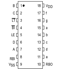
Features: • Low Logic Circuit Power Dissipation
• Highcurrent Sourcing Outputs (Up to 25 mA)
• Latch Storage of Binary Input
• Blanking Input
• Lamp Test Provision
• Readout Blanking on all Illegal Input Combinations
• Lamp Intensity Modulation Capability
• Time Share (Multiplexing) Capability
• Adds Ripple Blanking In, Ripple Blanking Out to MC14511B
• Supply Voltage Range = 3.0 V to 18 V
• Capable of Driving Two LowPower TTL Loads, One Lowpower Schottky TTL Load to Two HTL Loads Over
the Rated Temperature Range.
Pinout Specifications
|
Rating |
Symbol |
Value |
Unit |
| DC Supply Voltage |
VDD |
0.5 to + 18 |
V |
| Input Voltage, All Inputs |
Vin |
0.5 to VDD + 0.5 |
V |
| DC Current Drain per Input Pin |
I |
10 |
mA |
| Operating Temperature Range |
TA |
55 to + 125 |
|
| Power Dissipation, per Package† |
PD |
500 |
mW |
| Storage Temperature Range |
Tstg |
65 to + 150 |
|
Maximum Continuous Output Drive Current
(Source) per Output |
IOHmax |
25 |
mA |
Maximum Continuous Output Power
(Source) per Output ‡ |
POHmax |
50 |
mW |
‡POHmax = I
OH (V
DD V
OH)
* Maximum Ratings are those values beyond which damage to the device may occur.
†Temperature Derating:
Plastic "P and D/DW" Packages: 7.0 mW/ From 65 To 125
Ceramic "L" Packages: 12 mW/ From 100 To 125
DescriptionThe MC14513B BCDtoseven segment latch/decoder/driver is constructed with complementary MOS (CMOS) enhancement mode devices and NPN bipolar output drivers in a single monolithic structure. The MC14513B provides the functions of a 4bit storage latch, an 8421 BCDtoseven segment decoder, and has output drive capability. Lamp test (LT), blanking (BI), and latch enable (LE) inputs are used to test the display, to turnoff or pulse modulate the brightness of the display, and to store a BCD code, respectively. The Ripple Blanking Input (RBI) and Ripple Blanking Output (RBO) can be used to suppress either leading or trailing zeroes. MC14513B can be used with sevensegment light emitting diodes (LED), incandescent, fluorescent, gas discharge, or liquid crystal readouts either directly or indirectly.
Applications of MC14513B include instrument (e.g., counter, DVM, etc.) display driver, computer/calculator display driver, cockpit display driver, and various clock, watch, and timer uses.

 MC14513B Data Sheet


