MC14511B

Features: • Low Logic Circuit Power Dissipation• HighCurrent Sourcing Outputs (Up to 25 mA)• Latch Storage of Code• Blanking Input• Lamp Test Provision• Readout Blanking on all Illegal Input Combinations• Lamp Intensity Modulation Capability• Time Sh...

product image

MC14511B Picture
SeekIC No. : 004415375 Detail

MC14511B: Features: • Low Logic Circuit Power Dissipation• HighCurrent Sourcing Outputs (Up to 25 mA)• Latch Storage of Code• Blanking Input• Lamp Test Provision• Readout B...

floor Price/Ceiling Price

Part Number:
MC14511B
Supply Ability:
5000

Price Break

  • Qty
  • 1~5000
  • Unit Price
  • Negotiable
  • Processing time
  • 15 Days
Total Cost: $ 0.00

SeekIC Buyer Protection PLUS - newly updated for 2013!

  • Escrow Protection.
  • Guaranteed refunds.
  • Secure payments.
  • Learn more >>

Month Sales

268 Transactions

Rating

evaluate  (4.8 stars)

Upload time: 2024/11/27

Payment Methods

All payment methods are secure and covered by SeekIC Buyer Protection PLUS.

Notice: When you place an order, your payment is made to SeekIC and not to your seller. SeekIC only pays the seller after confirming you have received your order. We will also never share your payment details with your seller.
Product Details

Description


Features:

• Low Logic Circuit Power Dissipation
• HighCurrent Sourcing Outputs (Up to 25 mA)
• Latch Storage of Code
• Blanking Input
• Lamp Test Provision
• Readout Blanking on all Illegal Input Combinations
• Lamp Intensity Modulation Capability
• Time Share (Multiplexing) Facility
• Supply Voltage Range = 3.0 V to 18 V
• Capable of Driving Two Lowpower TTL Loads, One Lowpower Schottky TTL Load or Two HTL Loads Over the Rated Temperature Range
• Chip Complexity: 216 FETs or 54 Equivalent Gates
• Triple Diode Protection on all Inputs


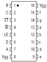
Pinout

  Connection Diagram


Specifications

CHARACTERISTIC
SYMBOL
RATING
UNIT
DC Supply Voltage
VDD
0.5 to + 18.0
V
Input or Output Voltage Range
VIN
0.5 to VDD + 0.5
    
V
DC Current Drain per Input Pin
I
10
mA
Operating Temperature Range
TA
    
55 to + 125
Power Dissipation
PD
500
mW
Storage Temperature Range
Tstg
-65to+ 150
Maximum Output Drive Current
(Source) per Output
IOHmax
25
mA
Maximum Continuous Output Power
(Source) per Output ‡
POHmax
50
mW
* Maximum Ratings are those values beyond which damage to the device may occur.


Description

The MC14511B BCDtoseven segment latch/decoder/driver is constructed with complementary MOS (CMOS) enhancement mode devices and NPN bipolar output drivers in a single monolithic structure. The MC14511B provides the functions of a 4bit storage latch, an 8421 BCDtoseven segment decoder, and an output drive capability. Lamp test (LT), blanking (BI), and latch enable (LE) inputs are used to test the display, to turnoff or pulse modulate the brightness of the display, and to store a BCD code, respectively. MC14511B can be used with sevensegment lightemitting diodes (LED), incandescent, fluorescent, gas discharge, or liquid crystal readouts either directly or indirectly.

Applications of MC14511B include instrument (e.g., counter, DVM, etc.) display driver, computer/calculator display driver, cockpit display driver, and various clock, watch, and timer uses.


Customers Who Bought This Item Also Bought

Margin,quality,low-cost products with low minimum orders. Secure your online payments with SeekIC Buyer Protection.
Hardware, Fasteners, Accessories
Tapes, Adhesives
803
Semiconductor Modules
Power Supplies - Board Mount
Sensors, Transducers
View more