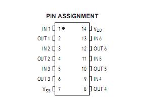
Features: • Supply Voltage Range = 3.0 Vdc to 18 Vdc• Capable of Driving Two LowPower TTL Loads or One LowPower Schottky TTL Load Over the Rated Temperature Range• Triple Diode Protection on All Inputs• PinforPin Replacement for CD4069UB• Meets JEDEC UB Specifications...
MC14069UB: Features: • Supply Voltage Range = 3.0 Vdc to 18 Vdc• Capable of Driving Two LowPower TTL Loads or One LowPower Schottky TTL Load Over the Rated Temperature Range• Triple Diode Pro...
SeekIC Buyer Protection PLUS - newly updated for 2013!
268 Transactions
All payment methods are secure and covered by SeekIC Buyer Protection PLUS.
Symbol | Parameter | Value | Unit |
VDD | DC Supply Voltage Range | 0.5 to +18.0 | V |
Vin, Vout | Input or Output Voltage Range (DC or Transient) |
0.5 to VDD+0.5 | V |
Iin, Iout | Input or Output Current (DC or Transient) per Pin |
±10 | mA |
PD | Power Dissipation, per Package (Note 3.) |
500 | mW |
TA | Ambient Temperature Range | 55 to +125 | °C |
Tstg | Storage Temperature Range | 65 to +150 | °C |
TL | Lead Temperature (8Second Soldering) |
260 | °C |
The MC14069UB hex inverter is constructed with MOS Pchannel and Nchannel enhancement MC14069UB in a single monolithic structure. These inverters find primary use where low power dissipation and/or high noise immunity is desired. Each of the six inverters is a single stage to minimize propagation delays.