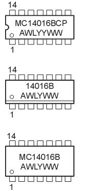
Features: Diode Protection on All InputsSupply Voltage Range = 3.0 Vdc to 18 VdcLinearized Transfer CharacteristicsLow Noise - 12 nV/Cycle, f 1.0 kHz typicalPinforPin Replacements for CD4016B, CD4066B (Note improvedtransfer characteristic design causes more parasitic couplingcapacitance than CD40...
MC14016B: Features: Diode Protection on All InputsSupply Voltage Range = 3.0 Vdc to 18 VdcLinearized Transfer CharacteristicsLow Noise - 12 nV/Cycle, f 1.0 kHz typicalPinforPin Replacements for CD4016B, CD40...
SeekIC Buyer Protection PLUS - newly updated for 2013!
268 Transactions
All payment methods are secure and covered by SeekIC Buyer Protection PLUS.
Symbol | Parameter | Value | Unit |
VDD | DC Supply Voltage Range |
0.5 to +18.0 |
V |
VIN , VOUT |
Input or Output Voltage Range (DC or Transient) |
0.5 to VDD + 0.5 |
V |
Iin | Input Current (DC or Transient) per Control Pin |
±10 |
mA |
ISW | Switch Through Current | ±25 |
mA |
PD | Power Dissipation, per Package (Note 3.) |
500 | mW |
TA | Ambient Temperature Range | 55 to +125 | |
Tstg | Storage Temperature Range | 65 to +150 | |
TL | Lead Temperature (8Second Soldering) |
260 |
The MC14016B quad bilateral switch is constructed with MOS Pchannel and Nchannel enhancement mode devices in a single monolithic structure. Each MC14016B consists of four independent switches capable of controlling either digital or analog signals. The quad bilateral switch is used in signal gating, chopper, modulator, demodulator and CMOS logic implementation.