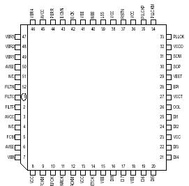
Application• SONET/SDHbased transmission systems, modules, test equipment• ATM using SONET• Add drop multiplexers• Other (nonSONET) data rate transmission systemsPinoutSpecifications Symbol Parameter Value Unit VCC, VCCO,VCCT, AVCC Power Supply (VEE, VEE...
MC10SX1405: Application• SONET/SDHbased transmission systems, modules, test equipment• ATM using SONET• Add drop multiplexers• Other (nonSONET) data rate transmission systemsPinoutSpecif...
SeekIC Buyer Protection PLUS - newly updated for 2013!
268 Transactions
All payment methods are secure and covered by SeekIC Buyer Protection PLUS.
US $4.26 - 6.3 / Piece
Counter Shift Registers 5V ECL 8-Bit Binary Up Synchronous
• SONET/SDHbased transmission systems, modules, test equipment
• ATM using SONET
• Add drop multiplexers
• Other (nonSONET) data rate transmission systems
Symbol |
Parameter |
Value |
Unit |
VCC, VCCO, VCCT, AVCC |
Power Supply (VEE, VEET, AVEE, GVEE = 0V) |
0.5 to +6.5 |
V |
VIN | Input Voltage (VEE, VEET, AVEE, GVEE = 0V) |
0.5 to +6.5 |
V |
IOUT | PECL Output Current Continuous Surge |
50 100 |
mA |
IOUTTTL | TTL Output Current |
5 |
mA |
TSTG | Storage Temperature |
50 to +175 |
°C |
Phase Locked Loop The onchip Phase Locked Loop (PLL) MC10SX1405 synthesizes the internal bit rate clock from the 19.44 / 38.66 / 77.78 MHz input reference clock. The PLL MC10SX1405 consists of a phase / frequency detector, loop filter, and Voltage Controlled Oscillator (VCO) nominally operating at 1.2 GHz. Dividers provide the internal clocks and a subrate clock output PLLCKP/PLLCKM (differential PECL) for phase comparison.
REFCK/REFCKM MC10SX1405 is the differential input PLL reference clock. The feedback, to close the loop of the PLL, is VARCK/VARCKM, the differential input variable clock. Both the REFCK and VARCK inputs of MC10SX1405 can be driven by TTL levels if the "minus" input (REFCKM and VARCKM) are left open.
An Out Of Lock indicator MC10SX1405 (OOL) is driven HIGH if the PLL is not frequency locked with the input reference clock.
Parallel to Serial Conversion In MC10SX1405OC3 mode, converts a 4bit (Nibble) 38.88 Mb/s or8bit (Byte) 19.44 Mb/s input to a differential 155.52 Mb/s serial data output. In OC12 mode, converts an 8bit 77.76 Mb/s input to a differential 622.08 Mb/s serial data output. The input data of MC10SX1405 is loaded into the Retime FF's by the Retiming Clock RETCK. Then the data is loaded into a shift register by PLLCK. The data shifted out is ordered MSB (DI1) first and LSB (DI8 or DI4) last.
Parity Check The parity check MC10SX1405 provides a means of verifying the integrity of the parallel to serial converter with minimal overhead. The parity of the serial output data stream is compared to the value of the Even Parity Input (EPI). If a parity error is deteced, the Parity Error (PERR) output is set HIGH. The PERR pin of MC10SX1405 has an Open Collector TTL Output and must be given a falling edge to reset the parity error detector.