Features: •3.2 Gb/s Typical Data Rate Capability•Differential Clock and Serial Outputs•VBB Output for Single-ended Input Applications•Asynchronous Data Reset (SYNC)•PECL Mode Operating Range:VCC= 3.0 V to 5.5 V with VEE= 0 V•NECL Mode Operating Range:VCC= 0 V wi...
MC10EP446: Features: •3.2 Gb/s Typical Data Rate Capability•Differential Clock and Serial Outputs•VBB Output for Single-ended Input Applications•Asynchronous Data Reset (SYNC)•PEC...
SeekIC Buyer Protection PLUS - newly updated for 2013!
268 Transactions
All payment methods are secure and covered by SeekIC Buyer Protection PLUS.
US $4.26 - 6.3 / Piece
Counter Shift Registers 5V ECL 8-Bit Binary Up Synchronous
Symbol | Parameter | Condition 1 | Condition 2 | Rating | Unit |
VCC | PECL Mode Power Supply | VEE= 0 V | 6 |
V | |
VEE | NECL Mode Power Supply | VCC= 0 V | −6 | V | |
VI | PECL Mode Input Voltage NECL Mode Input Voltage |
VEE= 0 V VCC= 0 V |
VI VCC VIVEE |
6 −6 |
V V |
Iout | Output Current | Continuous Surge |
50 100 |
mA mA | |
IBB | VBBSink/Source | ±0.5 | mA | ||
TA | Operating Temperature Range | −40 to +85 | °C | ||
Tstg | Storage Temperature Range | −65 to +150 | °C | ||
JA | Thermal Resistance (Junction−to−Ambient) | 0 lfpm 500 lfpm |
LQFP−32 LQFP−32 |
80 55 |
°C/W °C/W |
JC | Thermal Resistance (Junction−to−Case) | Standard Board | LQFP−32 | 12 to 17 | °C/W |
Tsol | Wave Solder | < 2 to 3 sec @ 248°C | 265 | °C |
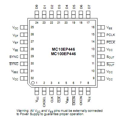
The MC10/100EP446 is an integrated 8−bit parallel to serial data converter. The MC10/100EP446 is designed with unique circuit topology to operate for NRZ data up to 3.2 Gb/s. The conversion sequence from parallel data into a serial data stream is from bit D0 to D7. The parallel input pins D0−D7 are configurable to bethreshold controlled by CMOS, ECL, or TTL level signals. The serial data rate output can be selected at internal clock data rate or twice the internal clocdata rateusing the CKSEL pin.
Control pins of MC10/100EP446 are provided to reset (SYNC) and disable internal clock circuitry (CKEN). In either CKSEL modes, the internal flip−flops are triggered on the rising edge for CLK and the multiplexers are switched on the falling edge of CLK, therefore, all associated specification limits are referenced to the negative edge of the clock input. Additionally, VBB pin is provided for single−ended input condition. The 100 Series devices contain temperature compensation network.