MC10EP445

Features: •300 ps Propagation Delay•5.0 Gb/s Typical Data Rate for CLKSEL LOW Mode•Differential Clock and Serial Inputs•VBBOutput for Single-Ended Input Applications•Asynchronous Data Synchronization (SYNC)•Asynchronous Master Reset (RESET)•PECL Mode Opera...

product image

MC10EP445 Picture
SeekIC No. : 004415036 Detail

MC10EP445: Features: •300 ps Propagation Delay•5.0 Gb/s Typical Data Rate for CLKSEL LOW Mode•Differential Clock and Serial Inputs•VBBOutput for Single-Ended Input Applications•As...

floor Price/Ceiling Price

Part Number:
MC10EP445
Supply Ability:
5000

Price Break

  • Qty
  • 1~5000
  • Unit Price
  • Negotiable
  • Processing time
  • 15 Days
Total Cost: $ 0.00

SeekIC Buyer Protection PLUS - newly updated for 2013!

  • Escrow Protection.
  • Guaranteed refunds.
  • Secure payments.
  • Learn more >>

Month Sales

268 Transactions

Rating

evaluate  (4.8 stars)

Upload time: 2024/11/27

Payment Methods

All payment methods are secure and covered by SeekIC Buyer Protection PLUS.

Notice: When you place an order, your payment is made to SeekIC and not to your seller. SeekIC only pays the seller after confirming you have received your order. We will also never share your payment details with your seller.
Product Details

Description


Features:

•300 ps Propagation Delay
•5.0 Gb/s Typical Data Rate for CLKSEL LOW Mode
•Differential Clock and Serial Inputs
•VBBOutput for Single-Ended Input Applications
•Asynchronous Data Synchronization (SYNC)
•Asynchronous Master Reset (RESET)
•PECL Mode Operating Range: VCC= 3.0 V to 5.5 Vwith VEE= 0 V
•NECL Mode Operating Range: VCC= 0 Vwith VEE= -3.0 V to -5.5 V
•Open Input Default State
•CLK ENABLE Immune to Runt Pulse Generation


Application

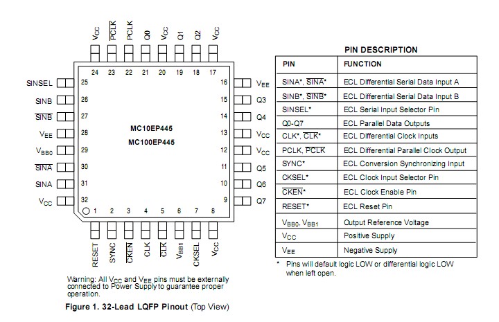
The MC10/100EP445 is an integrated 1:8 serial to parallel converter with two modes of operation selected by CKSEL (Pin 7). CKSEL HIGH mode only latches data on the rising edge of the input CLK and CKSEL LOW mode latches data on both the rising and falling edge of the input CLK. CKSEL LOW is the open default state. Either of the two differential input serial data path provided for this device,  SINA and SINB, can be chosen with the SINSEL pin (pin 25). SINA is the default input path when SINSEL pin is left floating. Because of internal pull-downs on the input pins, all input pins will default to logic low when left open.The two selectable serial data paths can be used for loop-back testing as well as the bit error testing. Upon power-up, the internal flip-flops will attain a random state. To synchronize multiple flipflops in the device,  the Reset (pin 1) must be asserted. The reset pin will disable the internal clocksignalirrespective of the CKEN state (CKEN disables the internal clock circuitry). The device will grab the first stream of data after the falling edgeof RESET


Pinout

  Connection Diagram


Specifications

Symbol


Parameter

Condition 1

Condition 2

Rating

Unit
VCC PECL Mode Power Supply VEE= 0 V   6 V
VEE NECL Mode Power Supply VCC= 0 V   -6 V
VI PECL Mode Input Voltage
NECL Mode Input Voltage
VEE= 0 V
VCC= 0 V

VIVCC

VIVEE

6
-6
V
V
IOUT Output Current Continuous
Surge
  50
100
mA
mA
IBB VBBSink/Source     ±0.5 mA
TA Operating Temperature Range     -40 to +85
Tstg Storage Temperature Range     -65 to+150
0JA Thermal Resistance (Junction-to-Ambient) 0 LFPM
500 LFPM
32 LQFP
32 LQFP
80
55
/W
/W
0JC Thermal Resistance (Junction-to-Case) std bd 32 LQFP 12 to 17 /W
Tsol Wave Solder < 2 to 3sec@248°C   265


Description

The MC10/100EP445 is an integrated 8bit differential serial to parallel data converter with asynchronous data synchronization. The MC10/100EP445 has two modes of operation. CKSEL HIGH mode is designed to operate NRZ data rates of up to 3.3 Gb/s, while CKSEL LOW mode is designed to operate at twice the internal clock data rate of up to5.0 Gb/s. The conversion sequence was chosen to convert the first serial bit to Q0, the second bit to Q1, etc. Two selectable differential serial inputs, which are selected by SINSEL, provide this device with loop-back testing capability. The MC10/100EP445 has a SYNC pin which, when held high for at least two consecutive clock cycles, will swallow one bit of data shifting the start of the conversion data fromD n to Dn+1. Each additional shift requires an additional pulse to be applied to the SYNC pin. Control pins are provided to reset and disable internal clock circuitry. Additionally, VBB  pin is provided for single-ended input condition.

The 100 Series contains temperature compensation. 


Customers Who Bought This Item Also Bought

Margin,quality,low-cost products with low minimum orders. Secure your online payments with SeekIC Buyer Protection.
Line Protection, Backups
Integrated Circuits (ICs)
Batteries, Chargers, Holders
Static Control, ESD, Clean Room Products
Inductors, Coils, Chokes
Circuit Protection
View more