Features: •Maximum Frequency > 1.0 GHz Typical
•50 ps Output−to−Output Skew
•PECL Mode Operating Range: VCC = 3.0 V to 5.5 V with VEE = 0 V
•NECL Mode Operating Range: VCC = 0 V with VEE = −3.0 V to −5.5 V
•Open Input Default State
•Safety Clamp on Inputs
•Synchronous Enable/Disable
•Master Reset for Synchronization of Multiple Chips
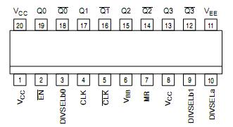
•VBB OutputPinout Specifications
Symbol
|
Parameter
|
Condition 1
|
Condition 2
|
Rating
|
Unit |
| VCC |
PECL Mode Power Supply |
VEE= 0 V |
|
6 |
V |
| VEE |
NECL Mode Power Supply |
VCC= 0 V |
|
-6 |
V |
| VI |
PECL Mode Input Voltage
NECL Mode Input Voltage |
VEE= 0 V
VCC= 0 V |
VIVCC
VIVEE
|
6
-6 |
V
V |
| IOUT |
Output Current |
Continuous
Surge |
|
50
100 |
mA
mA |
| IBB |
VBBSink/Source |
|
|
±0.5 |
mA |
| TA |
Operating Temperature Range |
|
|
-40 to +85 |
|
| Tstg |
Storage Temperature Range |
|
|
-65 to+150 |
|
| 0JA |
Thermal Resistance (Junction-to-Ambient) |
0 LFPM
500 LFPM |
TSSOP−20
TSSOP−20 |
90
60 |
/W
/W |
| 0JC |
Thermal Resistance (Junction-to-Case) |
Standard Board |
SOIC−20 |
33 to 35 |
/W |
| Tsol |
Wave Solder |
< 2 to 3sec@248°C |
|
265 |
|
DescriptionThe MC10/100EP139 is a low skew ÷2/4, ÷4/5/6 clock generation chip designed explicitly for low skew clock generation applications. The internal dividers are synchronous to each other, therefore, the common output edges are all precisely aligned. The MC10/100EP139 can be driven by either a differential or single−ended ECL or, if positive power supplies are used, LVPECL input signals. In addition, by using the VBB output, a sinusoidal source can be AC coupled into the device. If a single−ended input is to be used, the VBB output should be connected to theCLK input and bypassed to ground via a 0.01 F capacitor.
The common enable (EN )of MC10/100EP139 is synchronous so that the internal dividers will only be enabled/disabled when the internal clock is already in the LOW state. This avoids any chance of generating a runt clock pulse on the internal clock when the MC10/100EP139 is enabled/disabled as can happen with an asynchronous control. The internal enable flip-flop is clocked on the falling edge of the input clock, therefore, all associated specification limits are referenced to the negative edge of the clock input. Upon start-up, the internal flip-flops will attain a random state;therefore, for systems which utilize multiple EP139s, the master reset (MR) input of MC10/100EP139 must be asserted to ensure synchronization. For systems which only use one EP139, the MR pin need not be exercised as the internal divider design ensures synchronization between the ÷2/4 and the ÷4/5/6 outputs of a single device. All VCC and VEE pins must be externally connected to power supply to guarantee proper operation.
The 100 Series contains temperature compensation.

 MC10EP139 Data Sheet


