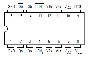
PinoutSpecifications Symbol Characteristic Min Typ Max Unit VSUP Total Supply Voltage|VEE| + |VCC| 12.0 V VPP Differential Input Voltage|V1 V2| 3.7 VDescriptionThe MC10E1652 is functionally and pin-for-pin compatible with the MC10E...
MC10E1652: PinoutSpecifications Symbol Characteristic Min Typ Max Unit VSUP Total Supply Voltage|VEE| + |VCC| 12.0 V VPP Differential Input Voltage|V1 V2| ...
SeekIC Buyer Protection PLUS - newly updated for 2013!
268 Transactions
All payment methods are secure and covered by SeekIC Buyer Protection PLUS.
US $4.26 - 6.3 / Piece
Counter Shift Registers 5V ECL 8-Bit Binary Up Synchronous
Symbol |
Characteristic |
Min |
Typ |
Max |
Unit |
VSUP |
Total Supply Voltage |VEE| + |VCC| |
12.0 |
V | ||
VPP |
Differential Input Voltage |V1 V2| |
3.7 |
V |
The MC10E1652 is functionally and pin-for-pin compatible with the MC10E1651 and thus the MC1651 in the MECL IIIE family, but is fabricated using Motorola's advanced MOSAIC IIIE process and is output compatible with 10H logic devices. In addition, the device is available in both a 16-pin DIP and a 20-pin surface mount package. However, the MC10E1652 provides user programmable hysteresis.
The latch enable (LENaand LENb) input pins operate from standard ECL 10HE logic levels. When the latch enable is at a logic high level the MC10E1652 acts as a comparator, hence Q will be at a logic high level if V1 > V2 (V1 is more positive than V2). Q is the complement of Q. When the latch enable input goes to a low logic level, the outputs of MC10E1652 are latched in their present state, providing the latch enable setup and hold time constraints are met. The level of input hysteresis is controlled by applying a bias voltage to the HYS pin.
• Typical 3.0 dB Bandwidth > 1.0 GHz
• Typical V to Q Propagation Delay of 775 ps
• Typical Output Rise/Fall of 350 ps
• Common Mode Range 2.0 V to +3.0 V
• Individual Latch Enables
• Differential Outputs
• Programmable Input Hysteresis