Features: • Maximum Frequency > 2 GHz Typical
• Fully Differential
• Advanced High Band Output Swing of 400 mV
• Theoretical Gain = 1.11
• Trise 97 ps Typical, Ffall 70 ps Typical
• The 100 Series Contains Temperature Compensation
• PECL Mode Operating Range: VCC = 3.0 V to 5.5 V with VEE = 0 V
• NECL Mode Operating Range: VCC = 0 V with VEE = −3.0 V to −5.5 V
• 50 Internal Termination Resistor
Pinout Specifications
|
Symbol |
Parameter |
Condition 1 |
Condition 2 |
Rating |
Units |
|
VCC |
PECL Mode Power Supply |
VEE = 0 V
|
|
6 |
V |
|
VEE |
NECL Mode Power Supply |
VCC = 0 V
|
|
-6 |
V |
|
VI |
PECL Mode Input Voltage
NECL Mode Input Voltage |
VEE = 0 V
VCC = 0 V
|
VI VCC
VI VEE
|
6
-6 |
V
V |
|
Iout |
Output Current |
Continuous
Surge
|
|
50
100 |
mA
mA |
|
IBB |
VBB Sink/Source
|
|
|
±0.5
|
mA |
|
TA |
Operating Temperature Range |
|
|
-40 to +85 |
|
|
Tstg |
Storage Temperature Range -65 to +150
|
|
|
-65 to +150 |
/W |
|
JA |
Thermal Resistance (Junction-to-Ambient) |
0 LFPM
500 LFPM |
20 TSSOP
20 TSSOP |
140
100 |
/W
/W
|
|
JC |
Thermal Resistance (Junction-to-Case) |
std bd |
20 TSSOP |
23 to 41 |
/W |
|
Tsol |
Wave Solder |
<2 to 3 sec @ 248
|
|
265 |
|
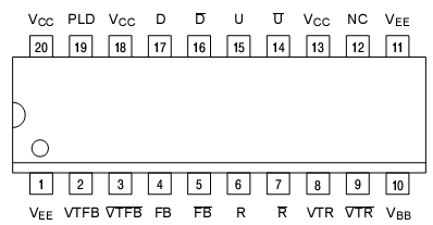
2. Maximum Ratings are those values beyond which device damage may occur.DescriptionThe MC100EP40 is a three-state phase-frequency detector intended for phase-locked loop applications which require a minimum amount of phase and frequency difference at lock. Advanced design significantly reduces the dead zone of the detector. For proper operation, the input edge rate of the R and V inputs should be less than 5 ns. The device is designed to work with a 3.3 V / 5 V power supply.
When Reference (R) and Feedback (FB) inputs are unequal in frequency and/or phase the differential UP (U) and DOWN (D) outputs will provide pulse streams which when subtracted and
integrated provide an error voltage for control of a VCO.
When Reference (R) and Feedback (FB) inputs are 80 ps or less in phase difference, the Phase Lock Detect pin will indicate lock by a high state (VOH). The VTX (VTR, VTR, VTFB, VTFB, ) pins offer an internal termination network for 50 line impedance environment shown in Figure 2. An external sinking supply of VCC-2 V is required on VTX pin(s). If you short the two differential VTR and VTR, (or VTFB and VTFB, ) together, you provide a 100 termination resistance that is compatible with LVDS signal receiver termination. For more information on termination of logic MC100EP40, see AND8020.
The VBB pin, an internally generated voltage supply, is available to this MC100EP40 only. For single-ended input conditions, the unused differential input is connected to VBB as a switching reference voltage. VBB may also rebias AC coupled inputs. When used, decouple VBB and VCC via a 0.01 F capacitor and limit current sourcing or sinking to 0.5 mA. When not used, VBB should be left open.
For more information on Phase Lock Loop operation, refer to AND8040.
Special considerations are required for differential inputs under No Signal conditions to prevent instability.

 MC100EP40 Data Sheet


