Features: · 500 ps Typical Propagation Delay · Maximum Frequency > 2.1 GHz Typical · Fully Differential Internally · Advanced High Band Output Swing of 400 mV · Transfer Gain:1.0 mV/Degree at 1.4 GHz 1.2 mV/Degree at 1.0 GHz · Rise and Fall Time: 100 ps Typical · The 100 Series Contains Tempera...
MC100EP140: Features: · 500 ps Typical Propagation Delay · Maximum Frequency > 2.1 GHz Typical · Fully Differential Internally · Advanced High Band Output Swing of 400 mV · Transfer Gain:1.0 mV/Degree at 1.4...
SeekIC Buyer Protection PLUS - newly updated for 2013!
268 Transactions
All payment methods are secure and covered by SeekIC Buyer Protection PLUS.
US $4.26 - 6.3 / Piece
Counter Shift Registers 5V ECL 8-Bit Binary Up Synchronous
· 500 ps Typical Propagation Delay
· Maximum Frequency > 2.1 GHz Typical
· Fully Differential Internally
· Advanced High Band Output Swing of 400 mV
· Transfer Gain:1.0 mV/Degree at 1.4 GHz 1.2 mV/Degree at 1.0 GHz
· Rise and Fall Time: 100 ps Typical
· The 100 Series Contains Temperature Compensation
· PECL Mode Operating Range: VCC = 3.0 V to 3.6 V with VEE= 0 V
· NECL Mode Operating Range: V CC= 0 V with VEE =-3.0 V to -3.6 V
· Open Input Default State
Symbol |
Parameter |
Condition 1 |
Condition 2 |
Rating |
Units |
VCC |
PECL Mode Power Supply | VEE = 0 V |
6 |
V | |
VEE |
NECL Mode Power Supply | V CC= 0 V |
-6 |
V | |
VI |
PECL Mode Input VoltagePECL Mode InutVoltage NECL Mode Input Voltage |
VEE = 0 V VCC = 0 V |
VIVCC VIvEE |
6 |
v v |
Iout |
Output Current | Continuous Surge |
50 100 |
mA mA | |
TA |
Operating Temperature Range |
-40 to +85 |
|||
Tstg |
Storage Temperature Range |
-65 to +150 |
|||
JA |
Thermal Resistance (Junction-to-Ambien | 0 LFPM 500 LFPM |
8 SOIC 8 SOIC |
190 130 |
/W |
JC |
Thermal Resistance (Junction-to-Case | std bd | 8 SOIC |
41 to 44 |
/W |
Tsol |
Wave Solder | <2 to 3 sec @ 248 |
265 |
The MC100EP140 is a three state phase frequency¤Cdetector intended fo phase¤Clocked loop applications which require a minimum amount of phas and frequency difference at lock. Since the part is designed with fully differential internal gates, the noise is reduced throughout the circuit, especially at high speeds. The basic operation of a Phase/Frequency Detector (PFD) is to !compare! an incoming signal (feedback) to a s reference signal. When the Reference (R) and Feedback (FB) inputs are unequal in frequency and/or phase, the differential UP (U) and DOWN (D) outputs will provide pulse streams which, when subtracted and integrated, provide an error voltage for control of a VCO. Detector states of operation are shown in the Figure 2 and the State Table.
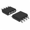
The MC100EP140 is packaged in a small outline, surface mount 8¤Clea SOIC package. The typical output amplitude of the EP140 is 400 mV, allowing faster switching time and greater bandwidth. For proper operation, the input edge rate of the R and FB inputs should be less than 5 ns.
More information on Phase Lock Loop operation and application can be found in AND8040.
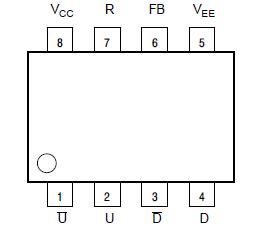
The pinout is shown in Figure 1, the logic diagram in Figure 3, and the typical termination in Figure 5.