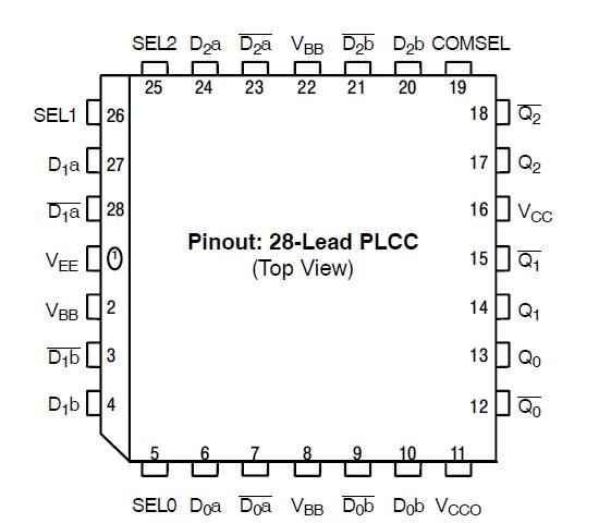
Features: • Differential D and Q; VBB available• 700 ps Max. Propagation Delay• High Frequency Outputs• Separate and Common Select• PECL Mode Operating Range: VCC = 4.2 V to 5.7 V with VEE = 0 V• NECL Mode Operating Range: VCC = 0 V with VEE = −4.2 V to ...
MC100E457: Features: • Differential D and Q; VBB available• 700 ps Max. Propagation Delay• High Frequency Outputs• Separate and Common Select• PECL Mode Operating Range: VCC = 4.2...
SeekIC Buyer Protection PLUS - newly updated for 2013!
268 Transactions
All payment methods are secure and covered by SeekIC Buyer Protection PLUS.
US $4.26 - 6.3 / Piece
Counter Shift Registers 5V ECL 8-Bit Binary Up Synchronous
Symbol |
Parameter |
Condition 1 |
Condition 2 |
Rating |
Unit |
VCC |
PECL Mode Power Supply |
VEE = 0 V |
8 |
V | |
VEE |
NECL Mode Power Supply |
VCC = 0 V |
−8 |
V | |
VI |
PECL Mode Input Voltage NECL Mode Input Voltage |
VEE = 0 V VCC = 0 V |
VI VCC VI VEE |
6 −6 |
V |
Iout |
Output Current |
Continuous Surge |
50 100 |
mA | |
IBB |
VBB Sink/Source |
± 0.5 |
mA | ||
TA |
Operating Temperature Range |
0 to +85 |
°C | ||
Tstg |
Storage Temperature Range |
−65 to +150 |
°C | ||
JA |
Thermal Resistance (Junction−to−Ambient) |
0 lfpm 500 lfpm |
PLCC−28 PLCC−28 |
63.5 43.5 |
°C/W °C/W |
JC |
Thermal Resistance (Junction−to−Case) |
Standard Board |
PLCC−28 |
22 to 26 |
°C/W |
Tsol |
Wave Solder Pb Pb−Free |
265 265 |
°C |
Stresses exceeding Maximum Ratings may damage the device. Maximum Ratings are stress ratings only. Functional operation above the Recommended Operating Conditions is not implied. Extended exposure to stresses above the Recommended Operating Conditions may affect device reliability.
The MC100E457 is a 3-bit differential 2:1 multiplexer. The fully differential data path makes the device ideal for multiplexing low skew clock or other skew sensitive signals.
The higher frequency outputs provide the device with a > 1.0 GHz bandwidth to meet the needs of the most demanding system clock. Both, separate selects and a common select, are provided to make the device well suited for both data path and random logic applications.
The differential inputs have internal clamp structures which will force the Q output of a gate in an open input condition to go to a LOW state. Thus, inputs of unused gates can be left open and will not affect the operation of the rest of the MC100E457. Note that the input clamp will take affect only if both inputs fall 2.5 V below VCC. The 100 Series contains temperature compensation.
Multiple VBB pins are provided to ease AC coupling input signals. The VBB pins, internally generated voltage supply pins, are available to this device only. For single-ended input conditions, the unused MC100E457 differential input is connected to VBB as a switching reference voltage. VBB may also rebias AC coupled inputs. When used, decouple VBB and VCC via a 0.01 F capacitor and limit current sourcing or sinking to 0.5 mA. When not used, VBB should be left open.