MC100E451

Features: • Differential Inputs: Data and Clock•VBBOutput•1100MHz Min. Toggle Frequency•Asynchronous Master Reset•Extended 100E VEERange of 4.2V to 5.46V•75kΩInput Pulldown ResistorsPinoutDescriptionTheMC100E451 contains six D-type flip-flops with single-e...

product image

MC100E451 Picture
SeekIC No. : 004414712 Detail

MC100E451: Features: • Differential Inputs: Data and Clock•VBBOutput•1100MHz Min. Toggle Frequency•Asynchronous Master Reset•Extended 100E VEERange of 4.2V to 5.46V•75k͐...

floor Price/Ceiling Price

Part Number:
MC100E451
Supply Ability:
5000

Price Break

  • Qty
  • 1~5000
  • Unit Price
  • Negotiable
  • Processing time
  • 15 Days
Total Cost: $ 0.00

SeekIC Buyer Protection PLUS - newly updated for 2013!

  • Escrow Protection.
  • Guaranteed refunds.
  • Secure payments.
  • Learn more >>

Month Sales

268 Transactions

Rating

evaluate  (4.8 stars)

Upload time: 2024/11/27

Payment Methods

All payment methods are secure and covered by SeekIC Buyer Protection PLUS.

Notice: When you place an order, your payment is made to SeekIC and not to your seller. SeekIC only pays the seller after confirming you have received your order. We will also never share your payment details with your seller.
Product Details

Description


Features:

• Differential Inputs: Data and Clock
•VBB Output
•1100MHz Min. Toggle Frequency
•Asynchronous Master Reset
•Extended 100E VEE Range of 4.2V to 5.46V
•75kΩ Input Pulldown Resistors


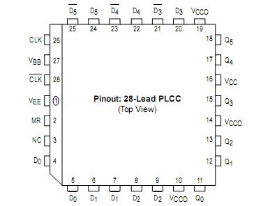
Pinout

  Connection Diagram


Description

The MC100E451 contains six D-type flip-flops with single-ended outputs and differential data inputs. The common clock input is alsodifferential. The registers are triggered by a positive transition of the positive clock (CLK) input.

A HIGH on the Master Reset (MR) input resets all Q outputs to LOW. The VBB output is intended for use as a reference voltage for single-ended reception of ECL signals to that device only. When using forthis purpose, it is recommended that VBB is decoupled to VCC via a0.0µF capacitor.
The differential input structures are clamped so that the inputs ofunused registers can be left open without upsetting the bias network of the MC100E451. The clamping action will assert the D and the CLK sides of theinputs. Because of the edge triggered flip-flop nature of the device simultaneously opening both the clock and data inputs will result in anoutput which reaches an unidentified but valid state. Note that the input clamps only operate when both inputs fall to 2.5V below VCC.


Customers Who Bought This Item Also Bought

Margin,quality,low-cost products with low minimum orders. Secure your online payments with SeekIC Buyer Protection.
Line Protection, Backups
Test Equipment
Circuit Protection
Optical Inspection Equipment
RF and RFID
View more