MB91F128

Features: • 32-bit RISC (FR30), load/store architecture, 5-step pipeline• Operating frequency : Internal 25 MHz• General register : 32bit x 16 registers• 16-bit fixed-length instructions (primitives), 1 instruction/1 cycle• Instructions of memory-to-memory transfer, b...

product image

MB91F128 Picture
SeekIC No. : 004413917 Detail

MB91F128: Features: • 32-bit RISC (FR30), load/store architecture, 5-step pipeline• Operating frequency : Internal 25 MHz• General register : 32bit x 16 registers• 16-bit fixed-length ...

floor Price/Ceiling Price

Part Number:
MB91F128
Supply Ability:
5000

Price Break

  • Qty
  • 1~5000
  • Unit Price
  • Negotiable
  • Processing time
  • 15 Days
Total Cost: $ 0.00

SeekIC Buyer Protection PLUS - newly updated for 2013!

  • Escrow Protection.
  • Guaranteed refunds.
  • Secure payments.
  • Learn more >>

Month Sales

268 Transactions

Rating

evaluate  (4.8 stars)

Upload time: 2024/11/27

Payment Methods

All payment methods are secure and covered by SeekIC Buyer Protection PLUS.

Notice: When you place an order, your payment is made to SeekIC and not to your seller. SeekIC only pays the seller after confirming you have received your order. We will also never share your payment details with your seller.
Product Details

Description


Features:

• 32-bit RISC (FR30), load/store architecture, 5-step pipeline
• Operating frequency : Internal 25 MHz
• General register : 32bit x 16 registers
• 16-bit fixed-length instructions (primitives), 1 instruction/1 cycle
• Instructions of memory-to-memory transfer, bit processing, and barrel shift : Instructions suitable for built-in
   control
• Function entry/exit instructions, multi load/store instruction for register data : High-level language compatible
   instructions
• Register interlock functions : Simple description of assembler language
• Branch instructions with delay slot : Reduced overhead on branching process
• Built-in multiplier/ Supporting at instruction level
   Signed 32-bit multiplying : 5 cycles
   Signed 16-bit multiplying : 3 cycles
• Interrupt (saving PC and PS) : 6 cycles, 16 priority levels
   Bus interface
• Maximum of 25 MHz internal operation rate
• 25-bit address bus (32 MB space)
• 16-bit address output, 8/16-bit data input/output
• Basic bus cycle : 2-clock cycle
• Chip selection outputs specifiable in a minimum of 64 Kbytes steps : 6 outputs
• Automatic wait cycle : Specifiable flexibly from 0 cycle to 7 cycles for each area
• Supporting time-division input/output interface for address/data (for area 1 only)
• Unassigned data/address terminals are available as input/output ports
• Supporting little endian mode (selecting one area from area 1 to area 5)
   DMAC (DMA controller)
• 8 channels
• Transfer factor : Interrupt request of built-in resources
• Transfer sequence : Step transfer/Block transfer/Burst transfer/Consecutive transfer
• Transfer data length : Selectable among 8 bits, 16 bits, and 32 bits
• Pausing is allowed by interrupt request
   UART
• 3 channels
• Full-duplex double buffer
• Data length : 7 to 9 bits (no parity), 6 to 8 bits (with parity)
• Asynchronous (start-stop synchronization) or CLK synchronous communication is selectable
• Multi processor mode
• Built-in 16-bit timer (U-Timer) used as a baud-rate generator : Generates an arbitrary baud rate
• External clock is available as a transfer clock
• Error detection : parity, frame, and overrun
   A/D converter (sequential transducer)
• 8/10-bit resolution, 8 channels
• Sequential comparison and transducer : At 25 MHz, 5.2 µs
• Built-in sample and hold circuit
• Conversion mode : Selectable among single conversion, scan conversion, and repeat conversion
• Activation : Selectable among software, external trigger, and built-in timer
   Reload timer
• 16-bit timer : 3 channels
• Internal clock : 2-clock cycle resolution, selectable among 2/8/32 dividing and external clock
Other interval timers
• 16-bit timer : 3 channels (U-Timer)
• PPG timer : 4 channels
• 16-bit OCU : 4 channels, ICU : 4 channels, Free-run timer : 1 channel
• Watchdog timer: 1 channel
Flash memory 510 KB
• 510 KB FLASH ROM: Read/Write/Erase is allowed with a same power
Built- in RAM 14 KB
• D-bus RAM 12 KB, C-bus RAM 2 KB
Bit search module
• Position of a first bit that changes between "1" and "0" is searched in one cycle, within an MSB of one word.
Interrupt controller
• External interrupt input : Normal interrupt*6 (INT0 to INT5)
• Internal interrupt factors : UART, DMAC, A/D, Reload timer, UTIMER, delay interrupt, PPG, ICU, and OCU
• Priority levels are programmable (16 levels)
Reset factors
• Power-on reset/watchdog timer/software reset/external reset
Low power consumption mode
• Sleep/stop mode
Clock control
• Built-in PLL circuit, selectable among 1-multiplication, and 2-multiplication
• Gearing function : Operation clock frequencies are freely and independently specifiable for CPU and
peripherals.
Gear clocks are selectable among 1/1, 1/2, 1/4, and 1/8 (or among 1/2, 1/4, 1/8, and 1/16).
Upper limit of peripheral operations is 25 MHz.
Others
• Package : LQFP-100
• CMOS technology : 0.35 µm
• Power supply voltage : 3.3 V±0.3 V


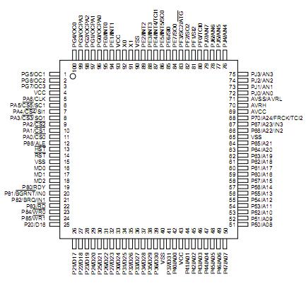
Pinout

  Connection Diagram


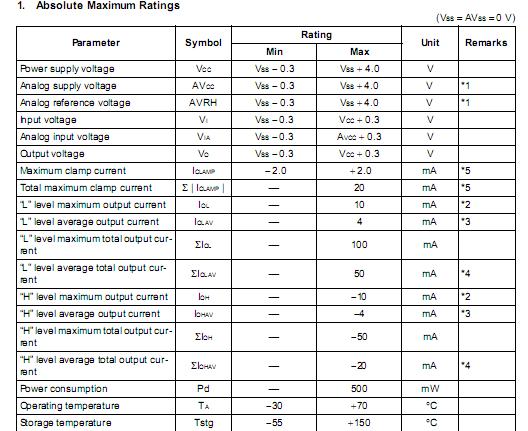
Specifications

  Connection Diagram
*1 : Care must be taken that AVCC, AVRH do not exceed VCC + 0.3 V. Also, care must be taken that AVRH do not
exceed AVCC.
*2 : Maximum output current defines a peak value of a specific terminal. 
*3 : Average output current defines a mean value of current flow within a period of 100 ms in a specific terminal. 
*4 : Average total output current defines a mean value of current flow within a period of 100 ms in all terminals. 
*5 :  • Aplicable to pins : D16 to D31, A00 to A24, RDY, BGRNT, BRQ, RD, WR0, WR1, CS0 to CS5, CLK, OCPA0
to OCPA3, OC0 to OC3, ALE, INT0 to INT5, SI0, SI2, SO0, SO2, TCI0, SC2
• Use within recommended operating conditions.
• Use at DC voltage (current) .
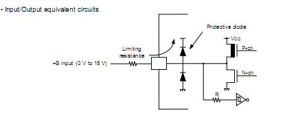
• The +B signal should always be applied with a limiting resistance placed between the +B signal and the
microcontroller.
• The value of the limiting resistance should be set so that when the signal is applied the input current to the
microcontroller pins does not exceed rated values, either instantaneously or for prolonged periods.
• Note that when the microcontroller drive current is low, such as in the power saving modes, the +B input
potential may pass through the protective diode and increase the potential at the VCC pin, and this may affect
other devices.
• Note that if a +B signal is input when the microcontroller power supply is off (not fixed at 0 V) , the power supply is
provided from the pins, so that incomplete operation may result.
• Note that if the +B input is applied during power-on, the power suplly is provided from the pins and the resulting
supply voltage may not be sufficient to operate the power-on reset.
• Care must be taken not to leave the input pin open.
• Sample recommended circuits
  Connection Diagram


Description

This model, designed on the basis of 32-bit RISC CPU (FR30 series), is a standard single-chip micro controller with built-in I/O resources and bus control functions. The functions are suitable for built-in control that requires high-speed CPU processing.
MB91F127 includes 256 Kbytes built-in flash memory and 14 Kbytes built-in RAM. MB91F128 includes 510 Kbytes
built-in flash memory and 14 Kbytes built-in RAM.
The specifications of MB91F128 are best suited for applications requiring high-level CPU processing capabilities,
such as navigation system, high-performance FAX, and printer controller.


Customers Who Bought This Item Also Bought

Margin,quality,low-cost products with low minimum orders. Secure your online payments with SeekIC Buyer Protection.
Tapes, Adhesives
803
Optoelectronics
Connectors, Interconnects
Cables, Wires - Management
View more