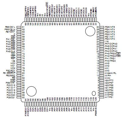
Features: • 32-bit RISC, load/store architecture, 5-stage pipeline
• Operating clock frequency: Internal 50 MHz/external 25 MHz (PLL used at source oscillation 12.5 MHz)
• General purpose registers: 32 bits * 16
• 16-bit fixed length instructions (basic instructions), 1 instruction/1 cycle
• Memory to memory transfer, bit processing, barrel shifter processing: Optimized for embedded applications
• Function entrance/exit instructions, multiple load/store instructions of register contents, instruction systems
supporting high level languages
• Register interlock functions, efficient assembly language coding
• Branch instructions with delay slots: Reduced overhead time in branch executions
• Internal multiplier/supported at instruction level
Signed 32-bit multiplication: 5 cycles
Signed 16-bit multiplication: 3 cycles
• Interrupt (push PC and PS): 6 cycles, 16 priority levels
Bus interface
• Clock doubler: Internal 50 MHz, external bus 25 MHz operation
• 25-bit address bus (32 Mbytes memory space)
• 8/16-bit data bus
• Basic external bus cycle: 2 clock cycles
• Chip select outputs for setting down to a minimum memory block size of 64 Kbytes: 8
• Interface supported for various memory technologies
DRAM interface (area 4 and 5)
• Automatic wait cycle insertion: Flexible setting, from 0 to 7 for each area
• Unused data/address pins can be configured us input/output ports
• Little endian mode supported (Select 1 area from area 1 to 5)
DRAM interface
• 2 banks independent control (area 4 and 5)
• Double CAS DRAM (normal DRAM I/F) / Single CAS DRAM / Hyper DRAM
• Basic bus cycle: Normally 5 cycles, 2-cycle access possible in high-speed page mode
• 2 way set associative
• 32 block/way, 4 entry(4 word)/block
• Lock function: For specific program code to be resident in cache memory
DMAC (DMA controller)
• 8 channels
• Transfer incident/external pins/internal resource interrupt requests
• Transfer sequence: Step transfer/block transfer/burst transfer/continuous transfer
• Transfer data length: 8 bits/16 bits/32 bits selective
• Internal clock: 2 clock cycle resolution, divide by 2/8/32 selective
Other interval timers
• 16-bit timer: 3 channels (U-TIMER)
• PWM timer: 4 channels
• Watchdog timer: 1 channel
Bit search module
First bit transition "1" or "0" from MSB can be detected in 1 cycle
Interrupt controller
• External interrupt input: Non-maskable interrupt (NMI), normal interrupt 8 (INT0 to INT7)
• Internal interrupt incident:UART, DMA controller (DMAC), A/D converter, U-TIMER and delayed interrupt
module
• Priority levels of interrupts are programmable except for non-maskable interrupt (in 16 levels)
Others
• Reset cause: Power-on reset/hardware standby/watchdog timer/software reset/external reset
• Low-power consumption mode: Sleep mode/stop mode
• Clock control
Gear function:Operating clocks for CPU and peripherals are independently selective
Gear clock can be selected from 1/1, 1/2, 1/4 and 1/8 (or 1/2, 1/4, 1/8 and 1/16)
However, operating frequency for peripherals is less than 25 MHz.
• Packages: LQFP-120
• CMOS technology (0.35 µm): MB91V108 (0.25 µm) ••••• Development model
MB91107 (0.25 µm) ••••• Production model
MB91108 (0.25 µm) ••••• Production model
• Power supply voltage: 3.3 V ± 0.3 V (internal regulator)Pinout Specifications
Parameter
|
Symbol |
Value |
Unit |
Remarks |
| Min. |
Max. |
| Power supply voltage |
VCC |
VSS − 0.3 |
VSS + 4.0 |
V |
*1 |
| Analog supply voltage |
AVCC |
VSS − 0.3 |
VSS + 4.0 |
V |
*2 |
| Analog reference voltage |
AVRH |
VSS − 0.3 |
VSS + 4.0 |
V |
*2 |
| Input voltage |
VI |
VSS − 0.3 |
VCC + 0.3 |
V |
|
| Analog pin input voltage |
VIA |
VSS − 0.3 |
AVCC + 0.3 |
V |
|
Output voltage
|
VO |
VSS − 0.3 |
VCC + 0.3 |
V |
|
| "L" level maximum output current |
IOL |
- |
10 |
mA |
*3 |
| "L" level average output current |
IOLAV |
- |
8
|
mA |
*4 |
| "L" level total maximum output current |
IOL |
- |
100 |
mA |
|
| "L" level total average output current |
IOLAV |
- |
50 |
mA |
*5 |
| "H" level maximum output current |
IOH |
- |
−10 |
mA |
*3 |
| "H" level average output current |
IOHAV |
- |
−4 |
mA |
*4 |
| "H" level total maximum output current |
IOH |
- |
−50 |
mA |
|
| "H" level total average output current |
IOHAV |
- |
−20 |
mA |
*5 |
| Power consumption |
PD
|
- |
500 |
mW |
|
| Operating temperature |
TA |
0 |
+70 |
°C
|
|
| Storage temperature |
Tstg |
-55 |
+150 |
°C |
|
DescriptionThe MB91108 is a standard single-chip microcontroller constructed around the 32-bit RISC CPU (FR* family)
core with abundant I/O resources and bus control functions optimized for high-performance/high-speed CPU
processing for embedded controller applications. To support the vast memory space accessed by the 32-bit CPU,
the MB91108 normally operates in the external bus access mode and executes instructions on the internal
1 Kbyte cache memory and RAM (MB91107: 128 Kbytes, MB91108: 160 Kbytes) for enhanced performance.
The MB91107 is optimized for applications requiring high-performance CPU processing such as navigation sys-
tems, high-performance FAXs and printer controllers.
*: FR Family stands for FUJITSU RISC controller.

 MB91108 Data Sheet


