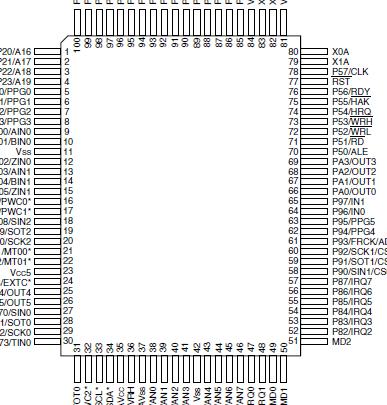
Features: • Clock
Minimum instruction execution time: 40.0 ns/6.25 MHz base frequency multiplied * 4 (25 MHz internal operating frequency/3.3 V ± 0.3 V) 62.5 ns/4 MHz base frequency multiplied * 4 (16 MHz internal operating frequency/3.0 V ± 0.3 V) PLL clock multiplier
• Maximum memory space: 16 Mbytes
• Instruction set optimized for controller applications Supported data types (bit, byte, word, or long word) Typical addressing modes (23 types) 32-bit accumulator for enhanced high-precision calculation Enhanced signed multiplication/division instruction and RETI instruction functions
• Instruction set designed for high-level programming language (C) and multi-task operations System stack pointer adopted
Instruction set symmetry and barrel shift instructions
• Non-multiplex bus/multiplex bus compatible
• Enhanced execution speed
4-byte instruction queue
• Enhanced interrupt functions
8 levels setting with programmable priority, 8 external interrupts
• Data transfer function (DMAC)
Up to 16 channels
• Embedded ROM
Flash versions : 192 Kbytes, 256 Kbytes, 384 Kbytes, MASK versions : 192 Kbytes, 256 Kbytes
• Embedded RAM
Flash versions : 4 Kbytes, 6 Kbytes, 10 Kbytes, 24 Kbytes, MASK versions : 10 Kbytes, 16 Kbytes
• General purpose ports
Up to 84 ports
(Includes 16 ports with input pull-up resistance settings, 16 ports with output open-drain settings)
• A/D converter
8-channel RC sequential comparison type (10-bit resolution, 3.68 s conversion time (at 25 MHz) )
• I2C interface (MB90485 series only) : 1channel, P76/P77 N-ch open drain pin (without P-ch) Do not apply high voltage in excess of recommended operating ranges to the N-ch open drain pin (with P-ch) in MB90V485B.
• PG (MB90485 series only) : 1 channel
• UART : 1 channel
• Extended I/O serial interface (SIO) : 2 channels
• 8/16-bit PPG : 3 channels (with 8-bit * 6 channel/16-bit * 3 channel mode switching function)
• 8/16-bit up/down counter/timer: 1 channel (with 8-bit * 2 channels/16-bit * 1-channel mode switching function)
• PWC (MB90485 series only) : 3 channels (Capable of compare the inputs to two of the three)
• 3 V/5 V I/F pin (MB90485 series only) P20 to P27, P30 to P37, P40 to P47, P70 to P77
• 16-bit reload timer : 1 channel
• 16-bit I/O timer : 2 channels input capture, 6 channels output compare, 1 channel free run timer
• On chip dual clock generator system
• Low-power consumption mode
With stop mode, sleep mode, CPU intermittent operation mode, watch mode, timebase timer mode
• Packages : QFP 100/LQFP 100
• Process : CMOS technology
• Power supply voltage : 3 V, single power supply (some ports can be operated by 5 V power supply at MB90485 series)
Pinout Specifications
| Parameter |
Symbol |
Rating |
Unit |
Remarks |
| Min |
Max |
| Power supply voltage*1 |
VCC3 |
VSS − 0.3 |
VSS + 4.0 |
V |
|
| VCC5 |
VSS − 0.3 |
VSS + 7.0 |
V |
|
| AVCC |
VSS − 0.3 |
VSS + 4.0 |
V |
*2 |
| AVRH |
VSS − 0.3 |
VSS + 4.0 |
V |
*2 |
| Input voltage*1 |
VI |
VSS − 0.3 |
VSS + 4.0 |
V |
*3 |
| VSS − 0.3 |
VSS + 7.0 |
V |
*3, *8, *9 |
| Output voltage*1 |
VO |
VSS − 0.3 |
VSS + 4.0 |
V |
*3 |
| VSS − 0.3 |
VSS + 7.0 |
V |
*3, *8, *9 |
| Maximum clamp current |
ICLAMP |
−2.0 |
+2.0 |
mA |
*7 |
| Total maximum clamp current |
ICLAMP |
- |
20 |
mA |
*7 |
| "L" level maximum output current |
IOL |
- |
10 |
mA |
*4 |
| "L" level average output current |
IOLAV |
- |
3 |
mA |
*5 |
| "L" level maximum total output current |
IOL |
- |
60 |
mA |
|
| "L" level total average output current |
IOLAV |
- |
30 |
mA |
*6 |
| "H" level maximum output current |
IOH |
- |
-10 |
mA |
*4 |
| "H" level average output current |
IOHAV |
- |
-3 |
mA |
*5 |
| "H" level maximum total output current |
IOH |
- |
-60 |
mA |
|
| "H" level total average output current |
IOHAV |
- |
-30 |
mA |
*6 |
| Power consumption |
PD |
- |
320 |
mW |
|
| Operating temperature |
TA |
-40 |
+85 |
°C |
|
| Storage temperature |
Tstg |
-55 |
+150 |
°C |
|
*1 : This parameter is based on VSS = AVSS = 0.0 V.
*2 : AVCC and AVRH must not exceed VCC. Also, AVRH must not exceed AVCC.
*3 : VI and V0 must not exceed VCC + 0.3 V. However, if the maximum current to/from and input is limited by some means with external components, the ICLAMP rating supersedes the VI rating.
*4 : Maximum output current is defined as the peak value for one of the corresponding pins.
*5 : Average output current is defined as the average current flow in a 100 ms interval at one of the corresponding pins.
*6 : Average total output current is defined as the average current flow in a 100 ms interval at all corresponding pins.
*7 : • Applicable to pins : P00 to P07, P10 to P17, P20 to P27, P30 to P37, P40 to P47, P50 to P57, P60 to P67,P70 to P77, P80 to P87, P90 to P97, PA0 to PA3
• Use within recommended operating conditions.
• Use at DC voltage (current) .
• The +B signal should always be applied with a limiting resistance placed between the +B signal and the icrocontroller.
• The value of the limiting resistance should be set so that when the +B signal is applied the input current to the microcontroller pin does not exceed rated values, either instantaneously or for prolonged periods.
• Note that when the microcontroller drive current is low, such as in the power saving modes, the +B input potential may pass through the protective diode and increase the potential at the VCC pin, and this may affect other devices.
• Note that if a +B signal is input when the microcontroller power supply is off (not fixed at 0 V) , the power supply is provided from the pins, so that incomplete operation may result.
• Note that if the +B input is applied during power-on, the power supply is provided from the pins and the resulting supply voltage may not be sufficient to operate the power-on reset.
• Care must be taken not to leave the +B input pin open.
• Note that analog system input/output pins other than the A/D input pins (LCD drive pins, comparator input pins, etc.) cannot accept +B signal input.
• Sample recommended circuits:
*8 : MB90485 series only P20 to P27, P30 to P37, P40 to P47, P70 to P77 pins can be used as 5 V I/F pin on applied 5 V to VCC5 pin.P76 and P77 is N-ch open drain pin.
*9 : As for P76 and P77 (N-ch open drain pin) , even if using at 3 V simplicity (VCC3 = VCC5) , the ratings are applied. WARNING: Semiconductor devices can be permanently damaged by application of stress (voltage, current,temperature, etc.) in excess of absolute maximum ratings. Do not exceed these ratings.
DescriptionThe MB90F481 series is a 16-bit general-purpose FUJITSU microcontroller designed for process control in consumer devices and other applications requiring high-speed real-time processing.
The F2MC-16LX CPU core instruction set retains the AT architecture of the F2MC*1 family, with additional instructions for high-level languages, expanded addressing mode, enhanced multiply-drive instructions, and complete bit processing. In addition, a 32-bit accumulator is provided to enable long-word processing. The MB90F481 series features embedded peripheral resources including 8/16-bit PPG, expanded I/O serial interface, UART, 10-bit A/D onverter, 16-bit I/O timer, 8/16-bit up/down-counter, PWC timer, I2C*2 interface, DTP/external interrupt, chip select, and 16-bit reload timer.
*1 : F2MC is the abbreviation for FUJITSU Flexible Microcontroller.
*2 : Purchase of Fujitsu I2C components conveys a license under the Philips I2C Patent Rights to use, these
components in an I2C system provided that the system conforms to the I2C standard a Specification as defined by Philips.

 MB90F481 Data Sheet


