Features: • Clock Embedded PLL clock multiplication circuit
Operating clock (PLL clock) can be selected from : divided-by-2 of oscillation or one to four times the oscillation
Minimum instruction execution time : 62.5 ns (operation at oscillation of 4 MHz, four times the oscillation clock,
VCC of 5.0 V)
VCC = 3.2 V to 5.5 V for MB90F548GL (S) /MB90547G (S) /548G (S)
Subsystem Clock : 32 kHz
• Instruction set to optimize controller applications Rich data types (bit, byte, word, long word) Rich addressing mode (23 types) Enhanced signed multiplication/division instruction and RETI instruction functions Enhanced precision calculation realized by the 32-bit accumulator
• Instruction set designed for high level language (C language) and multi-task operations Adoption of system stack pointer Enhanced pointer indirect instructions Barrel shift instructions
• Program patch function (for two address pointers)
• Enhanced execution speed : 4-byte Instruction queue
• Enhanced interrupt function : 8 levels, 34 factors
• Automatic data transmission function independent of CPU operation Extended intelligent I/O service function (EI2OS)
• Embedded ROM size and types
Mask ROM : 256 Kbytes / 64 Kbytes / 128 Kbytes
Flash ROM : 128 Kbytes/256 Kbytes
Embedded RAM size : 2 Kbytes/4 Kbytes/6 Kbytes/8 Kbytes (evaluation chip)
• Flash ROM Supports automatic programming, Embedded Algorithm TM* Write/Erase/Erase-Suspend/Resume commands A flag indicating completion of the algorithm Hard-wired reset vector available in order to point to a fixed boot sector in Flash Memory Erase can be performed on each block Block protection with external programming voltage
• Low-power consumption (stand-by) mode Sleep mode (mode in which CPU operating clock is stopped) Stop mode (mode in which oscillation is stopped) CPU intermittent operation mode Clock mode Hardware stand-by mode
• Process 0.5 m CMOS technology
• I/O port General-purpose I/O ports : 81 ports
• Timer Watchdog timer : 1 channel 8/16-bit PPG timer : 8/16-bit * 4 channels 16-bit re-load timer : 2 channels
• 16-bit I/O timer 16-bit free-run timer : 1 channel Input capture : 8 channels Output compare : 4 channels
• Extended I/O serial interface : 1 channel
• UART 0 With full-duplex double buffer (8-bit length) Clock asynchronized or clock synchronized (with start/stop bit) transmission can be selectively used.
• UART 1 With full-duplex double buffer (8-bit length) Clock asynchronized or clock synchronized serial (extended I/O serial) can be used.
• External interrupt circuit (8 channels) A module for starting an extended intelligent I/O service (EI2OS) and generating an external interrupt which is triggered by an external input.
• Delayed interrupt generation module
Generates an interrupt request for switching tasks.
• 8/10-bit A/D converter (8 channels) 8/10-bit resolution can be selectively used. Starting by an external trigger input. Conversion time : 26.3 s
• FULL-CAN interfaces
MB90540 series : 2 channel
MB90545 series : 1 channel
Conforming to Version 2.0 Part A and Part B
Flexible message buffering (mailbox and FIFO buffering can be mixed)
• External bus interface : Maximum address space 16 Mbytes
• Package: QFP-100, LQFP-100
* : Embedded Algorithm is a trade mark of Advanced Micro Devices Inc.
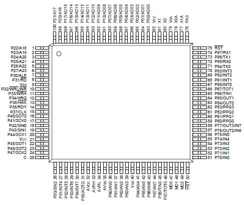
Pinout
Specifications
| Parameter |
Symbol |
Value |
Units |
Remarks |
| Min |
Max |
| Power supply voltage |
VCC |
VSS - 0.3 |
VSS + 6.0 |
V |
|
| AVCC |
VSS - 0.3 |
VSS + 6.0 |
V |
VCC = AVCC *1 |
AVRH,
AVRL |
VSS - 0.3 |
VSS + 6.0 |
V |
AVCC AVRH/AVRL,
AVRH AVRL *1 |
| Input voltage |
VI |
VSS - 0.3 |
VSS + 6.0 |
V |
*2 |
| Output voltage |
VO |
VSS - 0.3 |
VSS + 6.0 |
V |
*2 |
| Maximum clamp current |
ICLAMP |
- 2.0 |
+ 2.0 |
mA |
*6 |
| Total maximum clamp current |
| ICLAMP| |
- |
20 |
mA |
*6 |
| "L" level max output current |
IOL |
- |
15 |
mA |
*3 |
| "L" level avg. output current |
IOLAV |
- |
4 |
mA |
*4 |
| "L" level max overall output current |
IOL |
- |
100 |
mA |
|
| "L" level avg. overall output current |
IOLAV |
- |
50 |
mA |
*5 |
| "H" level max output current |
IOH |
- |
-15 |
mA |
*3 |
| "H" level avg. output current |
IOHAV |
- |
-4 |
mA |
*4 |
| "H" level max overall output current |
IOH |
- |
-100 |
mA |
|
| "H" level avg. overall output current |
IOHAV |
- |
-50 |
mA |
*5 |
| Power consumption |
PD |
- |
500 |
mW |
Flash device |
| - |
400 |
mW |
Mask ROM |
| Operating temperature |
TA |
-40 |
+85 |
°C |
MB90F543/F549 |
| -40 |
+105 |
°C |
Other than MB90F543/F549 |
| Storage temperature |
TSTG |
-55 |
+150 |
°C |
|
*1 : AVCC, AVRH, AVRL should not exceed VCC. Also, AVRH, AVRL should not exceed AVCC, and AVRL does not exceed AVRH.
*2 : VI and VO should not exceed VCC + 0.3 V. VI should not exceed the specified ratings. However if the maximum current to/from an input is limited by some means with external components, the ICLAMP rating supercedes the VI rating.
*3 : The maximum output current is a peak value for a corresponding pin.
*4 : Average output current is an average current value observed for a 100 ms period for a corresponding pin.
*5 : Total average current is an average current value observed for a 100 ms period for all corresponding pins.
*6 : ` Applicable to pins : P00 to P07, P10 to P17, P20 to P27, P30 to P37, P40 to P47, P50 to P57, P70 to P77, P80 to P87, P90 to P97, PA0
` Use within recommended operating conditions.
` Use at DC voltage (current) .
` The +B signal should always be applied with a limiting resistance placed between the +B signal and the microcontroller.
` The value of the limiting resistance should be set so that when the +B signal is applied the input current to the microcontroller pin does not exceed rated values, either instantaneously or for prolonged periods.
` Note that when the microcontroller drive current is low, such as in the power saving modes, the +B input potential may pass through the protective diode and increase the potential at the VCC pin, and this may affect other devices.
` Note that if a +B signal is input when the microcontroller current is off (not fixed at 0 V) , the power supply is provided from the pins, so that incomplete operation may result.
` Note that if the +B input is applied during power-on, the power supply is provided from the pins and the resulting supply voltage may not be sufficient to operate the power-on result.
DescriptionThe MB90540/545 series with FULL-CAN*1 and FLASH ROM is specially designed for automotive and industrial applications. Its main features are two on board CAN Interfaces (one for MB90V545 series) , which conform to V2.0 Part A and Part B, supporting very flexible message buffer scheme and so offering more functions than a normal full CAN approach. The instruction set by F2MC-16LX CPU core inherits an AT architecture of the F2MC*2 family with additional instruction sets for high-level languages, extended addressing mode, enhanced multiplication/ division instructions, and enhanced bit manipulation instructions.The micro controller has a 32-bit accumulator for processing long word data.The MB90540/545 series has peripheral resources of 8/10-bit A/D converters, UART (SCI) , extended I/O serial interfaces, 8/16-bit timer, I/O timer (input capture (ICU) , output compare (OCU) ) .
*1 : Controller Area Network (CAN) -License of Robert Bosch GmbH.
*2 : F2MC stands for FUJITSU Flexible Microcontroller.

 MB90545 Data Sheet


