Features: •Clock
Embedded PLL clock multiplication circuit
Operating clock (PLL clock) can be selected from : divided-by-2 of oscillation or one to four times the oscillation
Minimum instruction execution time : 62.5 ns (operation at oscillation of 4 MHz, four times the oscillation clock,
VCC of 5.0 V)
Subsystem Clock : 32 kHz
• Instruction set to optimize controller applications
Rich data types (bit, byte, word, long word)
Rich addressing mode (23 types)
Enhanced signed multiplication/division instruction and RETI instruction functions
Enhanced precision calculation realized by the 32-bit accumulator
• Instruction set designed for high level language (C language) and multi-task operations
Adoption of system stack pointer
Enhanced pointer indirect instructions
Barrel shift instructions
• Program patch function (for two address pointers)
• Enhanced execution speed : 4-byte Instruction queue
• Enhanced interrupt function : 8 levels, 34 factors
• Automatic data transmission function independent of CPU operation
Extended intelligent I/O service function (EI
2OS)
• Embedded ROM size and types
Mask ROM : 64 Kbytes / 128 Kbytes / 256 Kbytes
Flash ROM : 128 Kbytes/256 Kbytes
Embedded RAM size : 2 Kbytes/4 Kbytes/6 Kbytes/8 Kbytes (evaluation chip)
•Flash ROM
Supports automatic programming, Embedded Algorithm TM*
Write/Erase/Erase-Suspend/Resume commands
A flag indicating completion of the algorithm
Hard-wired reset vector available in order to point to a fixed boot sector in Flash Memory
Erase can be performed on each block
Block protection with external programming voltage
• Low-power consumption (stand-by) mode
Sleep mode (mode in which CPU operating clock is stopped)
Stop mode (mode in which oscillation is stopped)
CPU intermittent operation mode
Clock mode
Hardware stand-by mode
•Process
0.5 µm CMOS technology
• I/O port
General-purpose I/O ports : 81 ports
•Timer
Watchdog timer : 1 channel
8/16-bit PPG timer : 8/16-bit × 4 channels
16-bit re-load timer : 2 channels
• 16-bit I/O timer
16-bit free-run timer : 1 channel
Input capture : 8 channels
Output compare : 4 channels
• Extended I/O serial interface : 1 channel
•UART 0
With full-duplex double buffer (8-bit length)
Clock asynchronized or clock synchronized (with start/stop bit) transmission can be selectively used.
•UART 1
With full-duplex double buffer (8-bit length)
Clock asynchronized or clock synchronized serial (extended I/O serial) can be used.
• External interrupt circuit (8 channels)
A module for starting an extended intelligent I/O service (EI
2OS) and generating an external interrupt which
is triggered by an external input.
• Delayed interrupt generation module
Generates an interrupt request for switching tasks.
• 8/10-bit A/D converter (8 channels)
8/10-bit resolution can be selectively used.
Starting by an external trigger input.
Conversion time : 26.3 µs
• External bus interface : Maximum address space 16 Mbytes
• Package: QFP-100, LQFP-100
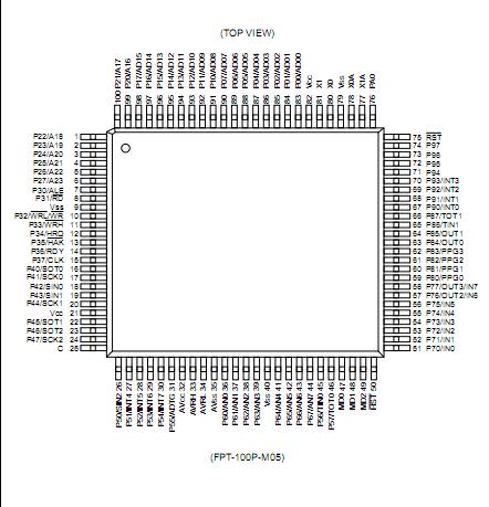
: Embedded Algorithm is a trade mark of Advanced Micro Devices Inc.Pinout Specifications
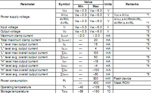
*1 : AVCC, AVRH, AVRL should not exceed VCC. Also, AVRH, AVRL should not exceed AVCC, and AVRL does not exceed AVRH.
*2 : VI and VO should not exceed VCC + 0.3 V. VI should not exceed the specified ratings. However if the maximum
current to/from an input is limited by some means with external components, the ICLAMP rating supercedes the VI rating.
*3 : The maximum output current is a peak value for a corresponding pin.
*4 : Average output current is an average current value observed for a 100 ms period for a corresponding pin.
*5 : Total average current is an average current value observed for a 100 ms period for all corresponding pins.
*6 : • Applicable to pins : P00 to P07, P10 to P17, P20 to P27, P30 to P37, P40 to P47, P50 to P57, P60 to P67,
P70 to P77, P80 to P87, P90 to P97, PA0
• Use within recommended operating conditions.
• Use at DC voltage (current) .
• The +B signal should always be applied with a limiting resistance placed between the +B signal and the
microcontroller.
• The value of the limiting resistance should be set so that when the +B signal is applied the input current to
the microcontroller pin does not exceed rated values, either instantaneously or for prolonged periods.
• Note that when the microcontroller drive current is low, such as in the power saving modes, the +B input
potential may pass through the protective diode and increase the potential at the VCC pin, and this may affect
other devices.
• Note that if a +B signal is input when the microcontroller current is off (not fixed at 0 V) , the power supply is
provided from the pins, so that incomplete operation may result.
• Note that if the +B input is applied during power-on, the power supply is provided from the pins and the
resulting supply voltage may not be sufficient to operate the power-on result.
• Care must be taken not to leave the +B input pin open.
• Note that analog system input/output pins other than the A/D input pins (LCD drive pins, comparator input
pins, etc.) cannot accept +B signal input.
• Sample recommended circuits :
DescriptionThe MB90438L (S) series with FLASH ROM is specially designed for industrial applications.
The instruction set by F2MC-16LX CPU core inherits an AT architecture of the F
2MC* family with additional instruction sets for high-level languages, extended addressing mode, enhanced multiplication/division instruc-tions, and enhanced bit manipulation instructions.The micro controller has a 32-bit accumulator for processing long word data.
The MB90438L (S) series has peripheral resources of 8/10-bit A/D converters, UART (SCI) , extended I/O serial
interfaces, 8/16-bit timer, I/O timer (input capture (ICU) , output compare (OCU) ) .
* : F
2MC stands for FUJITSU Flexible Microcontroller.

 MB90438L (S) Data Sheet


