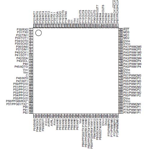
Features: • 16-bit core CPU; 4 MHz external clock (24 MHz internal, 42 ns instruction execution time)
• New 0.35 m CMOS Process Technology
• Internal voltage regulator supports 3 V MCU core, offering low EMI and low power consumption figures
• Up to five FULL-CAN interfaces; conforming to Version 2.0 Part A and Part B, flexible message buffering (mailbox and FIFO buffering can be mixed)
• Powerful interrupt functions (8 progr. priority levels; 8 external interrupts)
• EI2OS - Automatic transfer function indep.of CPU; 16 channels of intelligent I/O Services
• 18-bit Time-base counter
• Watchdog Timer
• 2 full duplex UARTs; support 10.4 Kbps (USA standard )
• Up to 2 full duplex UARTs (LIN/SCI)
• Serial I/O : 1 channel for synchronous data transfer
• Optional I2C* with 400 Kbps
• A/D Converter : 15 channels analog inputs (Resolution 10 bits or 8 bits)
• 16-bit reload timer * 2 channels
• ICU (Input capture) 16-bit * 6 channels (2 input pins are shared with OCU outputs)
• OCU (Output capture) 16-bit * 8 channels (2 output pins are shared with ICU input pins)
• 16-bit free running timer * 2 channels (FRT0 : ICU 0/1, OCU 0/1/2/3, FRT1 : ICU 2/3/4/5, OCU 4/5/6/7)
• 8/16-bit Programmable Pulse Generator 6 channels * 16-bit/12 channels * 8-bit
• Stepping Motor Controller 6 channels with slew rate controlled high current outputs
• Optimized instruction set for controller applications (bit, byte, word and long-word data types; 23 different addressing modes; barrel shift; variety of pointers)
• 4-byte instruction execution queue
• signed multiply (16-bit * 16-bit) and divide (32-bit/16-bit) instructions available
• Program Patch Function
• Fast Interrupt processing
• Low Power Consumption mode
Sleep mode
Timebase timer mode
Stop mode
CPU intermittent mode
• Sound Generator
• Real Time Watch Timer
• Built-In Clock Modulation circuit
• Programmable input levels (Automotive Hysteresis / CMOS Hysteresis, initial level is Automotive Hysteresis)
• Package : 120-pin plastic LQFP
Pinout Specifications
|
Parameter |
Symbol |
Min |
Max |
Unit |
Remarks |
| Power supply voltage |
VCC |
VSS - 0.3 |
VSS + 6.0 |
V |
|
|
AVCC |
VSS - 0.3 |
VSS + 6.0 |
V |
VCC = AVCC*2 |
|
AVRH,AVRL |
VSS - 0.3 |
VSS + 6.0 |
V |
AVCC AVRH, AVCC AVRL, AVRH AVRL |
|
DVCC |
VSS - 0.3 |
VSS + 6.0 |
V |
VCC DVCC |
| Input voltage |
VI |
VSS - 0.3 |
VCC + 0.3 |
V |
*3 |
| Output voltage |
VO |
VSS - 0.3 |
VCC + 0.3 |
V |
*3 |
| Maximum clamp current |
ICLAMP |
-40 |
+40 |
A |
*6 |
| Total maximum clamp current |
|ICLAMP| |
- |
4 |
mA |
*6 |
"L" level maximum
output current |
IOL1 |
- |
15 |
mA |
Normal outputs*4 |
|
IOL2 |
- |
40 |
mA |
High current outputs*5 |
"L" level average output
current |
IOLAV1 |
- |
4 |
mA |
Normal outputs, average value |
|
IOLAV2 |
- |
30 |
mA |
High current outputs, average value |
"L" level maximum
total output current |
IOL1 |
- |
100 |
mA |
Sum of all normal outputs |
|
IOL2 |
- |
330 |
mA |
Sum of all high current outputs |
"L" level average total
output current |
IOLAV1 |
- |
50 |
mA |
Sum of all normal outputs, average value |
|
IOLAV2 |
- |
250 |
mA |
Sum of all high current outputs,average value |
"H" level maximum
output current |
IOH1 |
- |
-15 |
mA |
Normal outputs*4 |
|
IOH2 |
- |
-40 |
mA |
High current outputs*5 |
"H" level average
output current |
IOHAV1 |
- |
-4 |
mA |
Normal outputs, average value |
|
IOHAV2 |
- |
-30 |
mA |
High current outputs, average value |
"H" level maximum
total output current |
IOH1 |
- |
-100 |
mA |
Sum of all normal outputs |
|
IOH2 |
- |
-330 |
mA |
Sum of all high current outputs |
"H" level average total
output current |
IOHAV1 |
- |
-50 |
mA |
Sum of all normal outputs, average value |
|
IOHAV2 |
- |
-250 |
mA |
Sum of all high current outputs,average value |
| Power consumption |
PD |
- |
800 |
mW |
MB90F394H(A)/MB90394HA |
| Operating temperature |
TA |
-40 |
+185 |
°C |
|
| Storage temperature |
TSTG |
-55 |
+150 |
°C |
|
*1 : The parameter is based on VSS = AVSS = DVSS = 0.0 V.
*2 : Set AVCC and VCC to the same voltage. Make sure that AVCC does not exceed VCC and that the voltage at the analog inputs does not exceed AVCC when the power is switched on.
*3 : VI and VO should not exceed VCC + 0.3 V. VI should not exceed the specified ratings. However if the maximum current to/from a input is limited by some means with external components, the ICLAMP rating supersedes the VI rating. For ports P70 to P77, P80 to P87 and PA0 to PA7, VI and VO should not exceed DVCC + 0.3 V.
*4 : Applicable to pins : P00 to P07, P10 to P17, P20 to P27, P30 to P37, P40 to P47, P50 to P57, P60 to P67,P90 to P97, PB0 to PB7
*5 : Applicable to pins : P70 to P77, P80 to P87, PA0 to PA7
*6 : • Applicable to pins : P00 to P07, P10 to P17, P20 to P27, P30 to P37, P40 to P47, P50 to P57, P60 to P67 P70 to P77, P80 to P87, P90 to P97, PA0 to PA7, PB0 to PB7
• Use within recommended operating conditions.
• Use at DC voltage (current)
• The +B signal should always be applied a limiting resistance placed between the +B signal and the microcontroller.
• The value of the limiting resistance should be set so that when the +B signal is applied the input current to the microcontroller pin does not exceed rated values, either instantaneously or for prolonged periods.
• Note that when the microcontroller drive current is low, such as in the power saving modes, the +B input potential may pass through the protective diode and increase the potential at the VCC pin, and this may affect other devices.
• Note that if a +B signal is input when the microcontroller power supply is off (not fixed at 0 V) , the power supply is provided from the pins, so that incomplete operation may result.
• Note that if the +B input is applied during power-on, the power supply is provided from the pins and the resulting supply voltage may not be sufficient to operate the power-on reset.
• Care must be taken not to leave the +B input pin open.
• Note that analog system input/output pins other than the A/D input pins (LCD drive pins, comparator input pins, etc.) cannot accept +B signal input.
DescriptionThe MB90390-series with up to five FULL-CAN* interfaces and Flash ROM is especially designed for automotive and industrial applications. Its main feature are up to five on board CAN Interfaces, which conform to V2.0 Part A and Part B, while supporting a very flexible message buffer scheme and so offering more functions than a normal full CAN approach. With the new 0.35 m CMOS technology, Fujitsu now offers on-chip Flash-ROM program memory up to 512 Kbytes. An internal voltage booster removes the necessity for a second programming voltage.
An on board voltage regulator provides 3 V to the internal MCU core. This creates a major advantage in terms of EMI and power consumption.
MB90390 provides an internal 42 ns instruction cycle time from an external 4 MHz clock.The unit features 6 Stepper Motor Controllers with slew rate controlled high current outputs.
Furthermore it features an 8-channel Output Compare Unit and a 6-channel Input Capture Unit with two separate 16-bit free running timers. Up to 4 UARTs constitute additional functionality for communication purposes.
* : Controller Area Network (CAN) - License of Robert Bosch GmbH

 MB90390 Data Sheet


