MB84VD2109X-85

Features: • Power supply voltage of 2.7 to 3.6 V• High performance 85 ns maximum access time• Operating Temperature -25 to +85 °C• Package 61-ball FBGA, 56-pin TSOP(I) 1. FLASH MEMORY• Simultaneous Read/Write operations (dual bank) Miltiple devices available with diff...

product image

MB84VD2109X-85 Picture
SeekIC No. : 004413505 Detail

MB84VD2109X-85: Features: • Power supply voltage of 2.7 to 3.6 V• High performance 85 ns maximum access time• Operating Temperature -25 to +85 °C• Package 61-ball FBGA, 56-pin TSOP(I) 1. FLA...

floor Price/Ceiling Price

Part Number:
MB84VD2109X-85
Supply Ability:
5000

Price Break

  • Qty
  • 1~5000
  • Unit Price
  • Negotiable
  • Processing time
  • 15 Days
Total Cost: $ 0.00

SeekIC Buyer Protection PLUS - newly updated for 2013!

  • Escrow Protection.
  • Guaranteed refunds.
  • Secure payments.
  • Learn more >>

Month Sales

268 Transactions

Rating

evaluate  (4.8 stars)

Upload time: 2024/11/27

Payment Methods

All payment methods are secure and covered by SeekIC Buyer Protection PLUS.

Notice: When you place an order, your payment is made to SeekIC and not to your seller. SeekIC only pays the seller after confirming you have received your order. We will also never share your payment details with your seller.
Product Details

Description


Features:

• Power supply voltage of 2.7 to 3.6 V
• High performance
   85 ns maximum access time
• Operating Temperature
   -25 to +85 °C
• Package 61-ball FBGA, 56-pin TSOP(I)
   1. FLASH MEMORY
• Simultaneous Read/Write operations (dual bank)
    Miltiple devices available with different bank sizes
    Host system can program or erase in one bank, then immediately and simultaneously read from the other bank
    Zero latency between read and write operations
    Read-while-erase
    Read-while-program
• Minimum 100,000 write/erase cycles
• Sector erase architecture
   Eight 4 K words and thirty one 32 K words.
   Any combination of sectors can be concurrently erased. Also supports full chip erase.
• Boot Code Sector Architecture
   MB84VD2108X : Top sector
   MB84VD2109X : Bottom sector
• Embedded EraseTM* Algorithms
    Automatically pre-programs and erases the chip or any sector
• Embedded ProgramTM* Algorithms
    Automatically writes and verifies data at specified address
• Data Polling and Toggle Bit feature for detection of program or erase cycle completion
• Ready-Busy output (RY/BY)
   Hardware method for detection of program or erase cycle completion
• Automatic sleep mode
   When addresses remain stable, automatically switch themselves to low power mode.
• Low VCCf write inhibit 2.5 V
• Hidden ROM (Hi-ROM) region
   64K byte of Hi-ROM, accessible through a new "Hi-ROM Enable" command sequence
   Factory serialized and protected to provide a secure electronic serial number (ESN)
• WP/ACC input pin
    At VIL, allows protection of boot sectors, regardless of sector protection/unprotection status
    (MB84VD2108X : SA37, SA38 MB84VD2109X : SA0, SA1)
    At VIH, allows removal of boot sector protection
    At VACC, program time will reduse by 40%.
• Erase Suspend/Resume
   Suspends the erase operation to allow a read in another sector within the same device
• Please refer to "MBM29DL16XTD/BD" data sheet in detailed function
   2. SRAM
• Power dissipation
   Operating: 50 mA max.
   Standby: 7 A max.
• Power down features using CE1s and CE2s
• Data retention supply voltage : 1.5 V to 3.6 V
• CE1s and CE2s Chip Select
• Byte data control : LBs (DQ0 to DQ7) , UBs (DQ8 to DQ15)
* : Embedded EraseTM and Embedded ProgramTM are trademarks of Advanced Micro Devices, Inc.


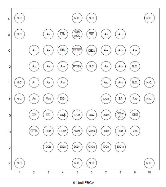
Pinout

  Connection Diagram


Specifications

Parameter Symbol Rating Unit
Min. Max.
Storage Temperature Tstg -55 +125 °C
Ambient Temperature with Power
Applied
TA -25 +85 °C
Voltage with Respect to Ground All
pins except A9, OE, RESET ,
WP/ACC (Note 1)
VIN, VOUT -0.3 VCCf +0.4 V
VCCs +0.4
VCCf/VCCs Supply (Note 1) VCCf, VCCs -0.3 +4.0 V
 A9 and OE (Note 2) VIN -0.3 +13.0 V
RESET (Note 2) VIN -0.5 +13.0 V
WP/ACC (Note 3) VIN -0.5 +10.5 V
WARNING: Semiconductor devices can be permanently damaged by application of stress (voltage, current,
                 temperature, etc.) in excess of absolute maximum ratings. Do not exceed these ratings.
Notes 1. Minimum DC voltage on input or I/O pins is 0.3 V. During voltage transitions, input or I/O pins may
              undershoot VSS to 2.0 V for periods of up to 20 ns. Maximum DC voltage on input or I/O pins is VCCf
              +0.4 V or VCCs+0.4 V. During voltage transitions, input or I/O pins may overshoot to VCCf+2.0 V or VCCs+2.0
              V for periods of up to 20 ns.
          2. Minimum DC input voltage on A9 and OE pin is 0.3 V. Minimum DC input voltage on RESET  pin is
             0.5 V. During voltage transitions, A9, OE, and RESET  pins may undershoot VSS to 2.0 V for periods of
              up to 20 ns.
              Voltage difference between input and supply voltage (VIN-VCCf or VCCs) does not exceed 9.0 V.
             Maximum DC input voltage on A9, OE, and RESET pins is +13.0 V which may overshoot to 14.0 V for
             periods of up to 20 ns.
         3. Minimum DC input voltage on WP/ACC pin is 0.5 V. During voltage transitions, WP/ACC pin may
             undershoot Vss to 2.0 V for periods of up to 20 ns. Maximum DC input voltage on WP/ACC pin is +10.5
             V which may overshoot to 12.0 V for periods of up to 20 ns, when VCCf is applied.


Customers Who Bought This Item Also Bought

Margin,quality,low-cost products with low minimum orders. Secure your online payments with SeekIC Buyer Protection.
Batteries, Chargers, Holders
Cables, Wires
Boxes, Enclosures, Racks
Connectors, Interconnects
Tapes, Adhesives
803
View more