MB81N643289-50

Features: • Double Data Rate• Bi-directional Data Strobe Signal• Eight bank operation• Burst read/write operation• Programmable, burst length, and CAS latency• Write latency (Write command to data input) = CAS latency -1• Byte write control by DM0 to DM3&#...

product image

MB81N643289-50 Picture
SeekIC No. : 004413464 Detail

MB81N643289-50: Features: • Double Data Rate• Bi-directional Data Strobe Signal• Eight bank operation• Burst read/write operation• Programmable, burst length, and CAS latency• Wr...

floor Price/Ceiling Price

Part Number:
MB81N643289-50
Supply Ability:
5000

Price Break

  • Qty
  • 1~5000
  • Unit Price
  • Negotiable
  • Processing time
  • 15 Days
Total Cost: $ 0.00

SeekIC Buyer Protection PLUS - newly updated for 2013!

  • Escrow Protection.
  • Guaranteed refunds.
  • Secure payments.
  • Learn more >>

Month Sales

268 Transactions

Rating

evaluate  (4.8 stars)

Upload time: 2024/11/27

Payment Methods

All payment methods are secure and covered by SeekIC Buyer Protection PLUS.

Notice: When you place an order, your payment is made to SeekIC and not to your seller. SeekIC only pays the seller after confirming you have received your order. We will also never share your payment details with your seller.
Product Details

Description


Features:

• Double Data Rate
• Bi-directional Data Strobe Signal
• Eight bank operation
• Burst read/write operation
• Programmable, burst length, and
   CAS latency
• Write latency (Write command to data input)
    = CAS latency -1
• Byte write control by DM0 to DM3
• Page Close Power Down Mode
• Distributed Auto-refresh cycle in 8 ms
• 2.5 V CMOS Source Termination I/O
   for all signals
• VDD: +2.5V Supply ± 0.2V tolerance
• VDDQ: +2.5V Supply ± 0.2V tolerance


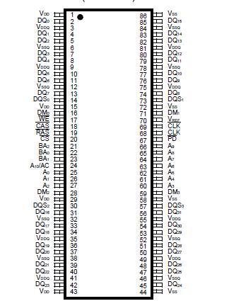
Pinout

  Connection Diagram


Specifications

Parameter Symbol Value Unit
Voltage of VCC Supply Relative to VSS VDD, VDDQ 0.5 to +3.6 V
Voltage at Any Pin Relative to VSS VIN, VOUT 0.5 to +3.6 V
Short Circuit Output Current IOUT ±50 mA
Power Dissipation PD 2.0 W
Storage Temperature TSTG 55 to +125 °C

WARNING: Semiconductor devices can be permanently damaged by application of stress (voltage, current,
                  temperature, etc.) in excess of absolute maximum ratings. Do not exceed these ratings.


Description

The Fujitsu MB81N643289-50 is a CMOS Fast Cycle Random Access Memory (FCRAM) containing 67,108,864 memory cells accessible in an 32-bit format. The MB81N643289-50 features a fully synchronous operation referenced to clock edge whereby all operations are synchronized at a clock input which enables high performance and simple user interface coexistence. The MB81N643289 is designed to reduce the complexity of using a standard dynamic RAM (DRAM) which requires many control signal timing constraints. The MB81N643289-50 uses Double Data Rate (DDR) where data bandwidth is twice of fast speed compared with regular SDRAMs.

The MB81N643289-50 is designed using Fujitsu advanced FCRAM Core Technology.

The MB81N643289-50 is ideally suited for Digital Visual System, High Performance Graphic Adapters, Hardware Accelerators, Buffers, and other applications where large memory density and high effective bandwidth are required and where a simple interface is needed.

The MB81N643289-50 adopts new I/O interface circuitry, 2.5 V CMOS Source Termination I/O interface, which is capable of extremely fast data transfer of quality under point to point bus environment.


Customers Who Bought This Item Also Bought

Margin,quality,low-cost products with low minimum orders. Secure your online payments with SeekIC Buyer Protection.
Motors, Solenoids, Driver Boards/Modules
Prototyping Products
DE1
Crystals and Oscillators
Inductors, Coils, Chokes
Sensors, Transducers
Fans, Thermal Management
View more