Features: · Low Power Dissipation: 1.15W/Channel (typ)
· High Speed: 500Mbps at 3VP-P
· Programmable 35mA Active-Load Current
· Low Timing Dispersion
· Wide -1.5V to +6.5V Operating Range
· Active Termination (3rd-Level Drive)
· Low Leakage Mode: 60nA
· Integrated Clamps
· Interfaces Easily with Most Logic Families
· Integrated PMU Connection
· Digitally Programmable Slew Rate
· Internal Termination Resistors
· Low Gain and Offset ErrorApplication· Low-Cost Mixed-Signal/System-on-Chip ATE
· Commodity Memory ATE
· PCI or VXI Programmable Digital InstrumentsPinout Specifications
VCC to GND.........................................................-0.3V to +11.5V
VEE to GND............................................................-7.0V to +0.3V
VCC - VEE................................................................-0.3V to +18V
GS to GND ..................................................................±1V
DUT_, LDH_, LDL_ to GND .....................................-2.5V to +7.5V
DATA_, NDATA_, RCV_, NRCV_,
LDEN_, NLDEN_ to GND.......................................-2.5V to +5.0V
DATA_ to NDATA_, RCV_ to NRCV_,
LDEN_ to NLDEN_......................................................±1.5V
VCCO_ to GND..........................................................-0.3V to +5V
SCLK, DIN, CS, RST, TDATA_,
TRCV_, TLDEN_ to GND .........................................-1.0V to +5V
DHV_, DLV_, DTV_, CHV_, CLV_, COM_,
FORCE_, SENSE_ to GND......................................-2.5V to +7.5V
CPHV_ to GND .....................................................-2.5V to +8.5V
CPLV_ to GND......................................................-3.5V to +7.5V
DHV_ to DLV_............................................................±10V
DHV_ to DTV_............................................................±10V
DLV_ to DTV_ ...........................................................±10V
CHV_ or CLV_ to DUT_..............................................±10V
CH_, NCH_, CL_, NCL_ to GND (open collector) ....-2.5V to +5V
CH_, NCH_, CL_, NCL_ to GND (open emitter) ..(VCCO_ + 1.0V)
All Other Pins to GND .....................(VEE - 0.3V) to (VCC + 0.3V)
Current Out of CH_, NCH_, CL_, NCL_ (open emitter) ...+50mA
DHV_, DLV_, DTV_, CHV_, CLV_,
CPHV_, CPLV_ Current.............................................±10mA
TEMP Current..................................................-0.5mA to +20mA
DUT_ Short Circuit to -1.5V to +6.5V.........................Continuous
Power Dissipation (TA = +70°C)
MAX9967_ _CCQ (derate 167mW/°C above +70°C) ...13.3W*
Storage Temperature Range .........................-65°C to +150°C
Junction Temperature.....................................................+125°C
Lead Temperature (soldering, 10s) .........................+300°C
*Dissipation wattage values are based on still air with no heat sink. Actual maximum allowable power dissipation is a function of heat extraction technique and may be substantially higher.
Stresses beyond those listed under "Absolute Maximum Ratings" may cause permanent damage to the evice.These are stress ratings only, and functional operation of the device at these or any other conditions beyond those indicated in the operational sections of the specifications is not implied. Exposure to absolute maximum rating conditions for extended periods may affect device reliability.
DescriptionThe MAX9967 dual, low-power, high-speed, pin electronics driver/comparator/load (DCL) IC includes, for each channel, a three-level pin driver, a dual comparator, variable clamps, and an active load. The driver MAX9967 features a wide voltage range and high-speed operation, includes high-impedance and active-termination (3rd-level drive) modes, and is highly linear even at low-voltage swings. The dual comparator MAX9967 provides low dispersion (timing variation) over a wide variety of input conditions. The clamps provide damping of high-speed device-undertest (DUT) waveforms when the device is configured as a high-impedance receiver. The programmable load of MAX9967 supplies up to 35mA of source and sink current. The load facilitates contact/continuity testing, at-speed parametric testing of IOH and IOL, and pullup of high-output-impedance devices.
The MAX9967A provides tight matching of gain and offset for the drivers, and offset for the comparators and active load, allowing reference levels to be shared across multiple channels in cost-sensitive systems. Use the MAX9967B for system designs that incorporate independent reference levels for each channel.
The MAX9967 provides high-speed, differential control inputs with optional internal termination resistors that are compatible with ECL, LVPECL, LVDS, and GTL. ECL/LVPECL or flexible open-collector outputs with optional internal pullup resistors are available for the comparators. These features significantly reduce the discrete component count on the circuit board.
A 3-wire, low-voltage, CMOS-compatible serial interface programs the low-leakage, slew-rate limit, and tristate/ terminate operational configurations of the MAX9967.
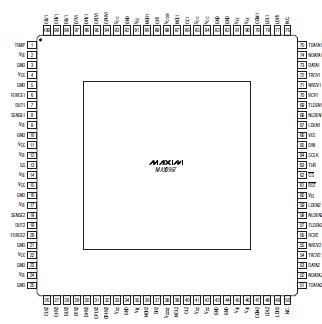
The MAX9967's operating range is -1.5V to +6.5V with power dissipation of only 1.15W per channel. The device is available in a 100-pin, 14mm x 14mm body, and 0.5mm pitch TQFP. An exposed 8mm x 8mm die pad on the top of the package facilitates efficient heat removal. The MAX9967 is specified to operate with an internal die temperature of +70°C to +100°C, and features a die temperature monitor output.

 MAX9967 Data Sheet


