Features: ·Small Footprint: Four Channels in 0.4in2
·Low Power Dissipation: 975mW/Channel (typ)
·High Speed: 500Mbps at 3VP-P
·Very Low Timing Dispersion
·Wide Operating Range: -1.5V to +6.5V
·Active Termination (3rd-Level Drive)
·Low-Leakage Mode: 15nA Maximum
·Integrated Clamps
·Interface Easily with Most Logic Families
·Digitally Programmable Slew Rate
·Internal Logic Termination Resistors
·Low Gain and Offset ErrorApplication·Memory Testers
·Low-Cost Mixed-Signal/System-on-Chip Testers
·Structural Testers
·Pattern/Data GeneratorsPinout Specifications
VCC to GND....................................................-0.3V to +11.5V
VEE to GND.......................................................-7.0V to +0.3V
All Other Pins ...............................(VEE - 0.3V) to (VCC + 0.3V)
VCC - VEE...........................................................-0.3V to +18V
DUT_ to GND....................................................-2.5V to +7.5V
DATA_, NDATA_, RCV_, NRCV_ to GND ..............-2.5 to +5.0V
DATA_ to NDATA_ .........................................................±1.5V
RCV_ to NRCV_.............................................................±1.5V
VCCO_ _ to GND.................................................-0.3V to +5V
SCLK, DIN, CS, RST to GND .................................-1.0V to +5V
DHV_, DLV_, DTV_, CHV_, CLV_ to GND ...........-2.5V to +7.5V
CPHV_ to GND ..................................................-2.5V to +8.5V
CPLV_ to GND...................................................-3.5V to +7.5V
DHV_ to DLV_.................................................................±10V
DHV_ to DTV_.................................................................±10V
DLV_ to DTV_ ................................................................±10V
CHV_ or CLV_ to DUT_...................................................±10V
CH_, NCH_, CL_, NCL_ to GND............................-2.5V to +5V
Current into DHV_, DLV_, DTV_,
CHV_, CLV_, CPHV_, CPLV_.....................................±10mA
Current into TEMP ........................................-0.5mA to +20mA
DUT_ Short Circuit to -1.5V to +6.5V .....................Continuous
Power Dissipation (TA = +70°C)
MAX9965__CCQ (derate 167mW/°C
above +70°C) .........................................................13.3W*
MAX9966__CCQ (derate 47.6mW/°C
above +70°C) ...........................................................3.8W*
Storage Temperature Range ......................-65°C to +150°C
Junction Temperature .................................................+125°C
Lead Temperature (soldering, 10s) .............................+300°C
*Dissipation wattage values are based on still air with no heat sink for the MAX9965 and slug soldered to board copper for the MAX9966. Actual maximum power dissipation is a function of users' heat extraction technique and may be substantially higher.
Stresses beyond those listed under "Absolute Maximum Ratings" may cause permanent damage to the device. These are stress ratings only, and functional operation of the device at these or any other conditions beyond those indicated in the operational sections of the specifications is not implied. Exposure to absolute maximum rating conditions for extended periods may affect device reliability.
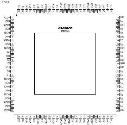
DescriptionThe MAX9965/MAX9966 four-channel, low-power, highspeed pin electronics driver and comparator ICs include for each channel a three-level pin driver, comparator,and variable clamps. The MAX9965/MAX9966 are similar to the MAX9963/MAX9964, but with even lower window comparator dispersion for enhanced accuracy. The driver MAX9965 features a wide voltage range and high-speed operation, includes high-Z and active termination (3rd-level drive) modes, and is highly linear even at low-voltage swings. The dual bipolar-input comparator provides very low dispersion (timing variation) over a wide variety of input conditions. The clamps of MAX9965 provide damping of high-speed DUT waveforms when the device is configured as a high-impedance receiver.
High-speed, differential control inputs of MAX9965 compatible with ECL, LVPECL, LVDS, and GTL levels are provided for each channel. ECL/LVPECL or flexible open-collector outputs are available for the comparators.
The A-grade version provides tight matching of gain and offset for the driver and comparator MAX9965, allowing reference levels to be shared across multiple channels in cost-sensitive systems. For system designs that incorporate independent reference levels for each channel,the B-grade version is available at reduced cost.
Optional internal resistors of MAX9965 at the high-speed inputs provide differential termination of LVDS inputs, while optional internal resistors provide the pullup voltage and source termination for open-collector comparator outputs. These features significantly reduce the discrete component count on the circuit board.
The MAX9965/MAX9966 operating range is -1.5V to +6.5V, with powerdissipation of only 975mW per channel.These devices are available in a 100-pin, 14mm x 14mm body, 0.5mm pitch TQFP with an exposed 8mm x 8mm die pad on the top (MAX9965) or bottom (MAX9966) of the package for efficient heat removal.
The MAX9965/MAX9966 are specified to operate with an internal die temperature of +60°C to +100°C, and feature a die temperature monitor output.

 MAX9965 Data Sheet


