`
` 3,8pF,600MHz
` 13V
` 12
`
Application
SOC
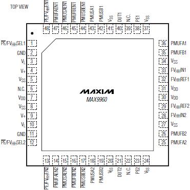
Pinout

Specifications
V+ to GND ..............................................................-0.3V to +26V
VDD to GND.........................................................-0.3V to +16.5V
VSS to GND............................................................-6.5V to +0.3V
VL to GND.................................................................-0.3V to +6V
V+ to VSS .............................................................................+32V
Digital Inputs.....................................(GND - 0.3V) to (VL + 0.3V)
FVHHIN_ ....................................................(the higher of -4V and
(VSS - 0.3V)) to (the lower of +10V and (VDD + 0.3V))
All Other Pins ...................................(VSS - 0.3V) to (VDD + 0.3V)
Continuous Current, PE_ ................................................±120mA
Continuous Current, PMUS_ _ ..........................................±10mA
Continuous Current, PMUFA_ + PMUFB_ +
(FVHH_ Path) ................................................................±45mA
Peak Current (100ns), PE_ .............................................±300mA
Peak Current (100ns), PMUS__ ........................................±20mA
Peak Current (100ns), PMUFA_ + PMUFB_ +
(FVHH_ Path) ................................................................±70mA
Package Continuous Power Dissipation (TA = +70°C)
48-Pin QFN-EP, on Single-Layer Board
(derate 27.8mW/°C above +70°C)..........................2222mW
48-Pin QFN-EP, on Multilayer Board
(derate 40.0mW/°C above +70°C)...........................3200mW
Operating Temperature Range..............................0°C to +70°C
Junction Temperature......................................................+150°C
Storage Temperature Range ...........................-65°C to +150°C
Lead Temperature (soldering 10s) ..................................+300°C
Stresses beyond those listed under "Absolute Maximum Ratings" may cause permanent damage to the device. These are stress ratings only, and functional operation of the device at these or any other conditions beyond those indicated in the operational sections of the specifications is not implied. Exposure to absolute maximum rating conditions for extended periods may affect device reliability.
Description
The MAX9960 dual-flash-pin electronics/supervoltage switch matrix replaces most of the relays and switches commonly needed to connect system resources to each of two pins in a flash memory or SOC ATE system (Figure 1). The device provides seven switches per channel to select up to four independent sources: the pin electronics (PE), two parametric measurement units (PMUs) or other Kelvin analog resources, and a flash memory programming supervoltage (FVHH_). The force-and-sense PMU switches are independently controlled, enabling their use to connect two non-Kelvin resources in place of each PMU or Kelvin resource. Each MAX9960 contains two complete seven-switch channels with fully independent controls.
The MAX9960 features signal path switches with wide 600MHz bandwidth, low 3 series resistance, and low 8pF shunt capacitance over a voltage range compatible with common pin electronics ICs. An on-chip voltage- doubling buffer with selectable 1x or 2x gain generates the flash supervoltage, allowing a 6.5V DAC reference input to generate up to a maximum of 13V for flash-memory programming levels.
When switching from the FVHH_ to PE_ or from PE_ to FVHH_, the device-under-test (DUT_) voltage behaves monotonically. Switching transitions between the PE_ and FVHH_ inputs are typically less than 350ns.
The MAX9960 operates over a commercial 0°C to +70°C temperature range, and is available in the 48-pin thin QFN package (7mm x 7mm x 0.8mm) with an exposed pad on the bottom for heat removal.

 MAX9960 Data Sheet


