Features: ` +1.7V to +3.3V (Digital) and +2.6V to +3.3V (Analog) Operation
` +2.6V to 5.5V Class D Speaker Amplifier Operation (Direct from Battery)
` Low 26mW Quiescent Power Consumption (Playback)
` High 98dB Power-Supply Rejection Ratio
` 8kHz to 48kHz Sample Rate (Replay and Record)
` Stereo 18-Bit ADC and DAC
` Low-Noise Stereo Microphone Inputs and Stereo Line Inputs
` Dual Source Digital Mixing (DAC)
` Selectable Voiceband Filter for Recording/Playback Modes
` Digital Filtering, Soft Mute, and Volume Control
` Low-Noise, High-PSRR Microphone Bias Generator
` Stereo DirectDrive Headphone Amplifier (2 x 50mW)
` Mono DirectDrive Handset Receiver Amplifier (1 x 10⁵mW)
` Stereo Class D, Ultra-Low-EMI, Filterless Speaker Amplifier with Active Emissions Limiting (2 x 1.25W, 8) (MAX9851)
` Stereo Differential Line Output Amplifiers (MAX9853)
` Clickless/Popless Operation
` Flexible Shutdown Modes for Power Saving
` Comprehensive Headset Detection
` Ultra-Low Power Wake-Up on Headset Detection
ApplicationGSM/GPRS/EDGE Cell Phones
PDAs/SmartPhonesPinout Specifications
(Voltages with respect to AGND)
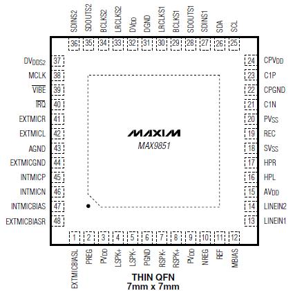
AVDD, DVDD, DVDDS2, CPVDD.................................-0.3V to +4V
PVSS, SVSS ...........................................................-4V to +0.3V
PVDD....................................................................-0.3V to +6V
AGND, DGND, CPGND, PGND.............................-0.3V to +0.3V
HPL, HPR, REC ..........................(SVSS - 0.3V) to (AVDD + 0.3V)
LSPK+, LSPK-, RSPK+, RSPK- ................-0.3V to (PVDD + 0.3V)
LINEIN1, LINEIN2...................................................-2V to +2V
EXTMICBIASL, EXTMICBIASR.................-0.3V to (AVDD + 0.3V)
INTMICP, INTMICN, EXTMICL, EXTMICR ..................-2V to +2V
EXTMICGND.......................................................-0.3V to +0.3V
C1N.......................................(PVSS - 0.3V) to (CPGND + 0.3V)
C1P....................................(CPGND - 0.3V) to (CPVDD + 0.3V)
PREG, REF, MBIAS, INTMICBIAS............-0.3V to (AVDD + 0.3V)
NREG....................................................+0.3V to (SVSS - 0.3V)
OUTL+, OUTL-, OUTR+, OUTR-,
FAULTIN.............................................-0.3V to (AVCC + 0.3V)
MCLK, IRQ, VIBE, SCL, SDA.................................-0.3V to +4V
SHDNOUT ...........................................................-0.3V to +6V
LRCLKS1, BCLKS1, SDOUTS1,
SDINS1...............................................-0.3V to DVDD + 0.3V
LRCLKS2, BCLKS2, SDOUTS2,
SDINS2 ..........................................-0.3V to DVDDS2 + 0.3V
Short Circuit to AGND Duration:
HPL, HPR, REC ...................................................Continuous
LSPK+, LSPK-, RSPK+,
RSPK- ..........Subject to Maximum Package Power Dissipation
INTMICBIAS, EXTMICBIASL, EXTMICBIASR..............Continuous
Short Circuit to AVDD Duration
EXTMICBIASL, EXTMICBIASR................................Continuous
Current Into/Out of Any Pin (unless otherwise noted)...100mA
Continuous Power Dissipation (TA = +70°C)
48-Pin Thin QFN (derate 40mW/°C above +70°C) ...3200mW
Junction Temperature......................................................+150°C
Operating Temperature Range .........................-40°C to +85°C
Storage Temperature Range ..........................-65°C to +150°C
Lead Temperature (soldering, 10s) ................................+300°C
Stresses beyond those listed under "Absolute Maximum Ratings" may cause permanent damage to the device. These are stress ratings only, and functional operation of the device at these or any other conditions beyond those indicated in the operational sections of the specifications is not implied. Exposure to absolute maximum rating conditions for extended periods may affect device reliability.
DescriptionThe MAX9851/MAX9853 are single-chip, stereo audio CODECs designed to provide a complete audio solution for a GSM/GPRS/EDGE cell phone. The MAX9851/MAX9853 provide stereo DirectDriveTM headphone amplifiers, a mono receiver speaker amplifier, stereo Class D speaker amplifiers (MAX9851 only), stereo differential line outputs (MAX9853 only), microphone input amplifiers, plus flexible input selection and gain control.Two serial digital audio interfaces are included, one intended to accept voiceband data and the other accepting I2S data. The MAX9851 voiceband interface can be reconfigured as needed to act as a secondary I2S feed input-allowing multiple audio source mixing of ringer tones or other audio at different sample rates. A transducer/ vibrator signal can be derived from digital audio.
The stereo digital-to-analog converter (DAC) path includes filtering and mixing, programmable-gain amplifiers (PGA), soft muting, and optional voiceband digital filtering. The MAX9851/MAX9853 accept up to two digital audio inputs at different sample rates. All analog inputs have PGAs on the front end, allowing dynamic range optimization with a wide range of input sources.
The stereo analog-to-digital converter (ADC) MAX9851 converts audio signals from either internal or external microphones or stereo line inputs. The microphone amplifiers have a programmable gain from 0 to 40dB to handle both amplified microphones and electret modules. In addition to a digital highpass filter to remove DC offset voltages, the ADC also features voiceband digital filtering.
The MAX9851 digital audio interfaces support a variety of serial audio formats. The secondary serial audio interface has an independent supply voltage to allow integration into multiple supply systems. Control for volume levels, signal mixing, and operating modes is done through the I2C† 2-wire interface.
All circuitry is optimized for high PSRR. The MAX9851/MAX9853 use a thermally efficient, space-saving 48-pin thin QFN package (7mm x 7mm x 0.8mm) with an exposed pad.

 MAX9851 Data Sheet


