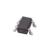
DescriptionThe MAX97200 is available in a tiny, 12-bump wafer level packaging (WLP 1.27mm x 1.65mm)with a small, 0.4mm lead pitch and specified over the -40°C to +85°C extended temperature range. The MAX97200 can be powered from a regulated 1.8V and have similar power consumption to a traditional DirectDrive amplifier that is powered from 0.9V. The MAX97200 is a 45mW Class H headphone amplifier that runs from a single low 1.8V supply voltage and employs Maxim's second-generation DirectDrivetechnology. When the output voltage is low, the power-supply voltage is QPVIN/2. When the output signal demands larger output voltage, the charge pump switches modes so that a greater power-supply voltage is realized and more output power can be delivered to the load. Second-generation DirectDrive technology improves power consumption when compared to first-generation DirectDrive amplifiers. Maxim's DirectDrive architecture uses an inverting charge pump to derive a negative voltage supply. The headphone amplifier is powered between the positive supply and the generated negative rail. The MAX97200 features a Dual ModeK internal charge pump to generate the power rails for the amplifier. The charge-pump output can be QPVIN/2 or QPVIN depending on the amplitude of the output signal. This scheme of MAX97200 allows the audio output signal to be biased about ground, eliminating the need for large DC-blocking capacitors between the amplifier output and the headphone load. Low-output offset voltage provides very good click-andpop performance both into and out of shutdown. High signal-to-noise ratio maintains system fidelity.
The features of MAX97200 can be summarized as (1)second-generation directdrive technology; (2)dynamic, class H, dual mode charge pump; (3)low voltage operation, VPVIN = 1.8V; (4)low quiescent current, 1.15mA (typ)at VPVIN = 1.8V; (5)eliminates large output DC-blocking capacitors; (6)industry-leading click-and-pop performance; (7)high-fidelity, SNR 105dB (5.6V output noise); (8)output power 34mW into 32I (THD+N 1%); (9)output power 45mW into 16I (THD+N 10%); (10)tiny, 12-bump, 1.27mm x 1.65mm (0.4mm lead pitch)WLP package.
The absolute maximum ratings of MAX97200 are (1)PVIN or PVDD to PGND: -0.3V to +2.2V; (2)GND to PGND: -0.3V to +0.3V; (3)PVSto PGND: -2.2V to +0.3V; (4)OUT_ and IN_ to GND: (PVS- 0.2V)to (PVDD + 0.2V); (5)C1P, C1N: cap connection only; (6)SHDN to GND: -0.3V to +4V; (7)output short-circuit current: continuous; (8)thermal limits multiple layer PCB continuous power dissipation (TA = +70°C)12-bump WLP (derate 13.7mW/°C above +70°C): 1095mW / 12-bump WLP JA: 73°C/W / 12-bump WLP BCA: 30°C/W; (9)junction temperature: +150°C; (10)operating temperature range: -40°C to +85°C; (11)storage temperature range: -65°C to +150°C; (12)bump temperature (soldering)reflow: +230°C.

 MAX97200 Data Sheet


