Features: ·Patented Spread-Spectrum Modulation Lowers Radiated Emissions
·Single-Supply Operation (2.5V to 5.5V)
·1.3W Stereo Output (8Ω, VDD = 5V, THD+N = 1%)
·No LC Output Filter Required
·87% Efficiency (RL = 8Ω, PO = 1000mW)
·Less Than 0.1% THD+N
·High 80dB PSRR
·Fully Differential Inputs
·Integrated Click-and-Pop Suppression
·Typical Low Quiescent Current (9mA)
·Typical Low-Power Shutdown Mode (0.1µA)
·Short-Circuit and Thermal-Overload Protection
·Available in Thermally Efficient, Space-Saving Packages
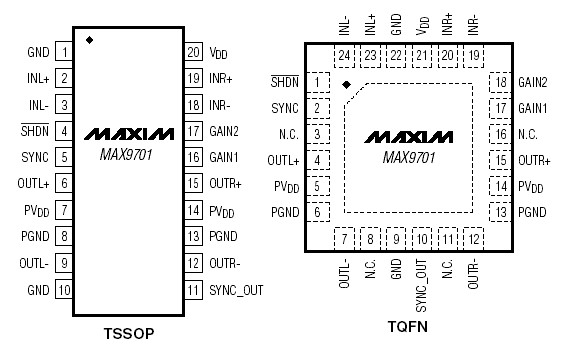
24-Pin Thin QFN-EP (4mm x 4mm x 0.8mm)
20-Pin TSSOP
20-Bump UCSP (2mm x 2.5mm x 0.6mm)Application·Cellular Phones
·Notebooks
·Handheld Gaming Consoles
·Docking Stations
·MP3 PlayersPinout SpecificationsVDD to GND.................................................................................6V
VDD to PVDD ............................................................-0.3V to +0.3V
PVDD to PGND ............................................................................6V
GND to PGND ...........................................................-0.3V to +0.3V
All Other Pins to GND.....................................-0.3V to (VDD + 0.3V)
Continuous Current In/Out of PVDD, PGND, OUT_............±800mA
Continuous Input Current (all other pins)...........................±20mA
Duration of OUT_ Short Circuit to GND or PVDD............Continuous
Duration of Short Circuit Between OUT+ and OUT- ......Continuous
Continuous Power Dissipation (TA = +70)
20-Bump UCSP (derate 10mW/ above +70) ................800mW
20-Pin TSSOP (derate 11mW/ above +70) ...............879.1mW
24-Pin Thin QFN (derate 20.8mW/ above +70) ......1666.7mW
Junction Temperature.........................................................+150
Operating Temperature Range ...............................-40 to +85
Storage Temperature Range ................................-65 to +150
Bump Temperature (soldering) Reflow...............................+235
Lead Temperature (soldering, 10s) ...................................+300DescriptionThe MAX9701 stereo class D audio power amplifier provides class AB amplifier audio performance with the benefits of class D efficiency, eliminating the need for a heatsink while extending battery life. The MAX9701 delivers up to 1.3W per channel into an 8Ω load while offering 87% efficiency. Maxim's next-generation, low- EMI modulation scheme allows the amplifier to operate without an external LC filter while still meeting FCC EMI emission levels.
The MAX9701 offers two modulation schemes: a fixed-frequency (FFM) mode, and a spread-spectrum (SSM) mode that reduces EMI-radiated emissions. The MAX9701 oscillator can be synchronized to an external clock through the SYNC input, allowing synchronization of multiple Maxim class D amplifiers. The sync output (SYNC_OUT) can be used for a master-slave application where more channels are required. The MAX9701 features a fully differential architecture, a full bridge-tied load (BTL) output, and comprehensive click-and-pop suppression. The device features internally set gains of 0dB, 6dB, 12dB, and 18dB selected through two gain-select inputs, further reducing external component count.
The MAX9701 features high 80dB PSRR, less than 0.1% THD+N, and SNR in excess of 88dB. Short-circuit and thermal-overload protection prevent the device from being damaged during a fault condition. The MAX9701 is available in 24-pin thin QFN-EP (4mm x 4mm x 0.8mm), 20-pin TSSOP, and 20-bump UCSP™ (2mm x 2.5mm x 0.6mm) packages. The MAX9701 is specified over the extended -40°C to +85°C temperature range.

 MAX9701 Data Sheet


