Features: · Five LVCMOS Outputs with Independent Frequency Selections
· One Buffered Reference Clock Output
· Eight Selectable Frequencies: 133, 125, 83, 66,62.5, 50, 33, and 25MHz
· Crystal or an Input-Clock-Based Clock Reference
· Output Frequency Programmed Through I2C Interface
· 0, -1.25%, or -2.5% Selectable Downspreading Rate
· Low Output Period Jitter (Without Spread Spectrum) < 10psRMS
· <220ps Output-to-Output Skew
· Available in 20-Lead, 5mm x 5mm, TQFN Package
· +3.3V Supply
· -40°C to +85°C Extended Temperature RangeApplicationNetwork Routers
Telecom/Networking Equipment
Storage Area Networks/Network Attached
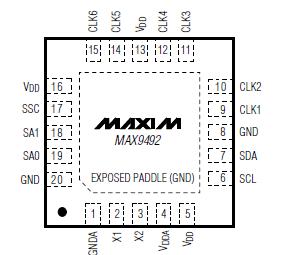
StoragePinout Specifications
VDD_ to GND .......................................................-0.3V to +4.0V
All Other Pins to GND.................................-0.3V to (VDD + 1.0V)
Short-Circuit Duration (all LVCMOS outputs) .............Continuous
ESD Protection (Human Body Model)................................. ±2kV
Continuous Power Dissipation (TA = +70°C)
20-Pin TQFN (derate 20.8mW/°C above +70°C) ......1667mW
Storage Temperature Range ..........................-65°C to +165°C
Maximum Junction Temperature .....................................+150°C
Operating Temperature Range .........................-40°C to +85°C
Lead Temperature (soldering, 10s) ................................+300°C
Stresses beyond those listed under "Absolute Maximum Ratings" may cause permanent damage to the device. These are stress ratings only, and functional operation of the device at these or any other conditions beyond those indicated in the operational sections of the specifications is not implied. Exposure to absolute maximum rating conditions for extended periods may affect device reliability.
DescriptionThe MAX9492 frequency synthesizer is designed to generate multiple clocks for clock distribution in network routers or switches. The device provides a total of six buffered clock outputs (CLK1 to CLK6). CLK1 of MAX9492 is the buffered output of the reference clock. CLK2 through CLK6 are independently programmable to generate eight different frequencies based on a 25MHz input crystal: 133, 125, 83, 66, 62.5, 50, 33, and 25MHz. All the outputs are LVCMOS single-ended signals. Either a 25MHz crystal or an external clock can serve as the input reference clock. The MAX9492 incorporates two phase-locked loops (PLLs) with two internal loop filters.
Select the MAX9492's output clock frequency by programming on-chip registers through the MAX9492's I2C* interface. The device also features spread-spectrum capability to reduce electromagnetic interference (EMI). This technique allows spreading the fundamental energy over a wider frequency range, hence reducing the respective energy amplitude. The output frequency spectrum is downspread by -1.25% or -2.5%.
The MAX9492 operates from a 3.3V supply and is guaranteed over the extended temperature range (-40°C to +85°C). The device is available in a space-saving,20-pin, TQFN, 5mm x 5mm package.

 MAX9492 Data Sheet


