Features: 8kHz Input Reference CLK
High-Jitter Rejection on the Reference CLK
Synthesizer Locks to the 8kHz Reference with a±200ppm Range
Output Frequency: 35.328MHz
Six Buffered LVTTL Low-Jitter Outputs
One 8kHz Reference CLK Relay Output
+3.3V Supply Operation
24-Pin TSSOP PackageApplicationTelecom Equipment Using T1, E1, T3, E3, and
ISDN Protocols
xDSL Equipment in CO with Interface to the
Telecom ProtocolsPinout Specifications
VDD to GND...........................................................-0.3V to +4.0V
VDDP to GNDP.......................................................-0.3V to +4.0V
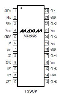
SHDN , REO, REIN, X1, X2, CLK_ to GND ...-0.3V to (VDD + 0.3V)
LP1, SETI to GNDP.......................................-0.3V to (VDD + 0.3V)
LP2 Internally Connected to GNDP
Short-Circuit Duration of Outputs ...............................Continuous
Continuous Power Dissipation (TA = +70°C)
24-Pin TSSOP (derate 12.2mW/°C above +70°C) ..........976mW
Operating Temperature Range .........................-40°C to +85°C
Maximum Junction Temperature .....................................+150°C
Storage Temperature Range ..........................-60°C to +150°C
ESD Rating (Human Body Model) ........................................±2kV
Lead Temperature (soldering, 10s) ................................+300°C
DescriptionThe MAX9486 low-cost, high-performance clock synthesizer with an 8kHz input reference clock provides six buffered LVTTL clock outputs at 35.328MHz. The clock synthesizer can be used to generate the clocks for T1,E1, T3, E3, and xDSL.
The MAX9486 has two phase-lock loops (PLLs). The first PLL uses a voltage-controlled crystal oscillator(VCXO). The second PLL is a frequency multiplier. With the two PLLs, the MAX9486 generates the output frequency at 35.328MHz. In addition, this device generates a jitter-suppressed 8kHz output that provides a better source for the reference clock relay.
The MAX9486 is available in a 24-pin TSSOP package and operates over the extended operating temperature range of -40°C to +85°C and a single +3V to +3.6V power-supply range.

 MAX9486 Data Sheet


