MAX9394

Features: · Guaranteed 1.5GHz Operation with 250mV Differential Output Swing· Simultaneous Loopback Control· 2ps(RMS) (max) Random Jitter· AC Specifications Guaranteed for 150mV Differential Input· Signal Inputs Accept Any Differential Signaling Standard· LVDS Outputs for Clock or High-Speed Data·...

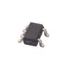
product image

MAX9394 Picture
SeekIC No. : 004412673 Detail

MAX9394: Features: · Guaranteed 1.5GHz Operation with 250mV Differential Output Swing· Simultaneous Loopback Control· 2ps(RMS) (max) Random Jitter· AC Specifications Guaranteed for 150mV Differential Input· ...

floor Price/Ceiling Price

Part Number:
MAX9394
Supply Ability:
5000

Price Break

  • Qty
  • 1~5000
  • Unit Price
  • Negotiable
  • Processing time
  • 15 Days
Total Cost: $ 0.00

SeekIC Buyer Protection PLUS - newly updated for 2013!

  • Escrow Protection.
  • Guaranteed refunds.
  • Secure payments.
  • Learn more >>

Month Sales

268 Transactions

Rating

evaluate  (4.8 stars)

Upload time: 2024/11/27

Payment Methods

All payment methods are secure and covered by SeekIC Buyer Protection PLUS.

Notice: When you place an order, your payment is made to SeekIC and not to your seller. SeekIC only pays the seller after confirming you have received your order. We will also never share your payment details with your seller.
Product Details

Description


Features:

· Guaranteed 1.5GHz Operation with 250mV Differential Output Swing
· Simultaneous Loopback Control
· 2ps(RMS) (max) Random Jitter
· AC Specifications Guaranteed for 150mV Differential Input
· Signal Inputs Accept Any Differential Signaling Standard
· LVDS Outputs for Clock or High-Speed Data
· High-Level Input Fail-Safe Detection (MAX9394)
· Low-Level Input Fail-Safe Detection (MAX9395)
· +3.0V to +3.6V Supply Voltage Range
· LVCMOS/LVTTL Logic Inputs


Application

High-Speed Telecom/Datacom Equipment
Central Office Backplane Clock Distribution
DSLAM
Protection Switching
Fault-Tolerant Systems


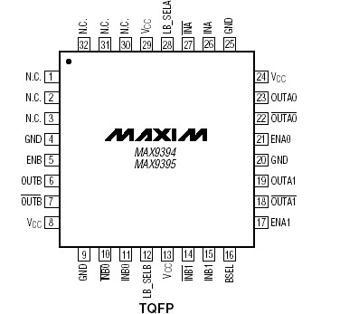
Pinout

  Connection Diagram


Specifications

VCC to GND...............................................................-0.3V to +4.1V
IN_ _, IN_ _, OUT_ _, OUT_ _, EN_ _, _SEL, LB_SEL_
to GND............................................................-0.3V to (VCC + 0.3V)
IN_ _ to IN_ _...........................................................................±3V
Short-Circuit Duration (OUT_ _, OUT_ _) .......................Continuous
Continuous Power Dissipation (TA = +70).
   32-Pin TQFP (derate 13.1mW/ above +70)...............1047mW
   28-Pin 5mm x 5mm Thin QFN
   (derate 20.8mW/ above +70)...................................1667mW
Junction-to-Ambient Thermal Resistance in Still Air
   32-Pin TQFP..................................................................+76.4/W
   28-Pin 5mm x 5mm Thin QFN............................................+48/W
Junction-to-Case Thermal Resistance
   28-Pin 5mm x 5mm Thin QFN..............................................+2/W
Operating Temperature Range ..................................-40 to +85
Junction Temperature.............................................................+150
Storage Temperature Range ....................................-65 to +150
ESD Protection (Human Body Model)
   (IN_ _, IN_ _, OUT_ _, OUT_ _, EN_ _, SEL_, LB_SEL_) ........±2kV
Soldering Temperature (10s) ................................................+300

Stresses beyond those listed under "Absolute Maximum Ratings" may cause permanent damage to the device. These are stress ratings only, and functional operation of the device at these or any other conditions beyond those indicated in the operational sections of the specifications is not implied. Exposure to absolute maximum rating conditions for extended periods may affect device reliability.


Description

The MAX9394/MAX9395 consist of a 2:1 multiplexer and a 1:2 demultiplexer with loopback. The multiplexer section (channel B) accepts two low-voltage differential signaling (LVDS) inputs and generates a single LVDS output. The demultiplexer section (channel A) accepts a single LVDS input and generates two parallel LVDS outputs. The MAX9394/MAX9395 feature a loopback mode that connects the input of channel A to the output of channel B and connects the selected input of channel B to the outputs of channel A.

Three LVCMOS/LVTTL logic inputs of MAX9394 control the internal connections between inputs and outputs, one for the multiplexer portion of channel B (BSEL), and the other two for loopback control of channels A and B (LB_SELA and LB_SELB). Independent enable inputs for each differential output pair provide additional flexibility.

Fail-safe circuitry of MAX9394 forces the outputs to a differential low condition for undriven inputs or when the commonmode
voltage exceeds the specified range. The MAX9394 provides high-level input fail-safe detection for HSTL, LVDS, and other GND-referenced differential inputs. The MAX9395 provides low-level fail-safe detection for CML, LVPECL, and other VCC-referenced differential inputs.

Ultra low 91psP-P (max) pseudorandom bit sequence (PRBS) jitter ensures reliable communications in highspeed links that are highly sensitive to timing error, especially those incorporating clock-and-data recovery, or serializers and deserializers. The high-speed switching performance guarantees 1.5GHz operation and less than 87ps (max) skew between channels.

LVDS inputs and outputs are compatible with the TIA/EIA-644 LVDS standard. The LVDS outputs drive 100Ω loads. The MAX9394/MAX9395 are offered in 32- pin TQFP and 28-pin thin QFN packages and operate over the extended temperature range (-40 to +85).


Customers Who Bought This Item Also Bought

Margin,quality,low-cost products with low minimum orders. Secure your online payments with SeekIC Buyer Protection.
Power Supplies - Board Mount
Integrated Circuits (ICs)
Boxes, Enclosures, Racks
RF and RFID
Computers, Office - Components, Accessories
View more